Analyzing Intel-Micron 3D XPoint: The Next Generation Non-Volatile Memory
by Kristian Vättö, Ian Cutress & Ryan Smith on July 31, 2015 11:00 AM ESTEstimating 3D XPoint Die Size
By now most of you probably know that I'm a sucker for die sizes and since this is information that the DRAM and NAND vendors are unwilling to share, I've gone as far as developing my own method for estimating the die size (well, it's really just primary school geometry, so I can't take too much credit for it). Die size is the key factor in determining cost efficiency because it directly relates to the number of gigabytes each wafer yields and thus it's a vital metric for comparing different technologies and process nodes.
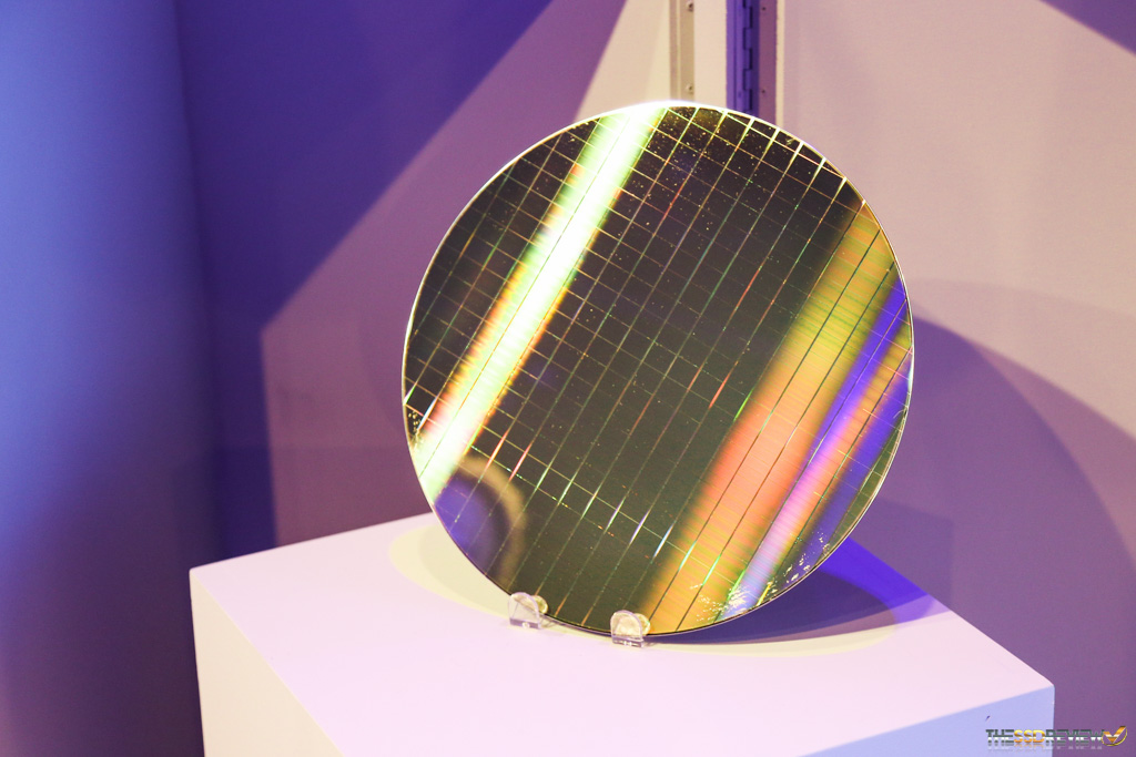
I'm borrowing the above picture from The SSD Review because to be honest my wafer photos (and photos in general) are quite horrible and wafers are far from being the easiest object given all the reflections. Sean is a professional photographer, so he managed to grab this clear and beautiful photo of the production 3D XPoint wafer Intel and Micron had on display, making it easy to estimate the die size.
I calculated 18 dies horizontally and 22 vertically, which yields 227mm^2 with a normal 300mm wafer. When taking die cuts (i.e. the space between dies) into account, we should be looking at 210-220mm^2. Array efficiency is about 90%, which is much higher than planar NAND because most of the peripheral circuitry lies underneath the memory array.
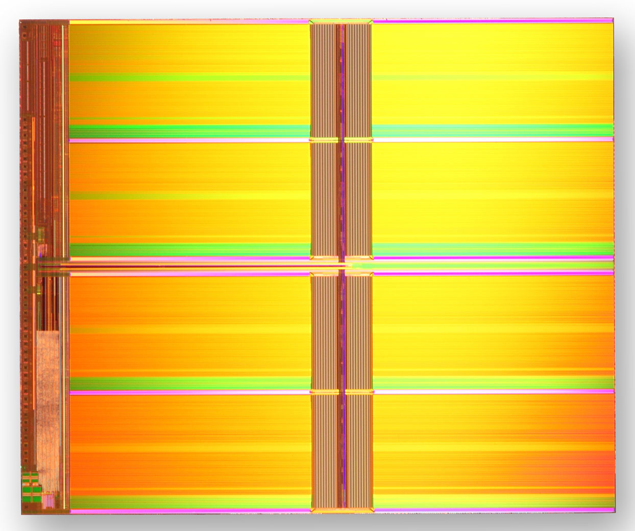
IMFT 20nm 128Gbit MLC NAND die
For comparison, Intel-Micron's 20nm 128Gbit MLC NAND die measures 202mm^2 and has array efficiency of ~75%. From that we can calculate that the 128Gbit memory array in 3D XPoint takes about 190mm^2, while a similar capacity planar NAND array measures ~150mm^2 (since the 128Gbit 3D XPoint die consists of two layers and 128Gbit MLC NAND die stores two bits per cell, the number of layers and bits stored per cell cancel out). It seems like NAND is denser (about 20-25%) from a memory array perspective given a fixed feature size (i.e. lithography), but at this point it's hard to say whether this is due to the cell design itself or something else. Connecting layers of wordlines and bitlines to the intermetal layers likely takes some extra area compared to a 2D process (at least this is the case with 3D NAND), which might partially explain the lower density compared to NAND.
However we will have to wait for some SEM photos to really see what's happening inside the 3D XPoint array and how it compares to NAND in cell size and overall density efficiency. Of course, there is a lot more in total manufacturing cost than just the cell and die size, but I'll leave the full analysis to those with the proper equipment and deeper knowledge of semiconductor manufacturing processes.
What Happens to 3D NAND
The above analysis already gives a hint that 3D XPoint isn't about to replace 3D NAND, at least not in the foreseeable future. That's also what Intel and Micron clearly stated when asked about 3D XPoint's impact on 3D NAND because it's really a new class of memory that fills a niche that DRAM and NAND cannot. The companies are still looking forward to rolling out 3D NAND next year and have a strong roadmap of future 3D NAND generations.
As I mentioned earlier, the way 3D XPoint array is built is quite different from 3D NAND and my understanding is that it's less economical, which is one of the reasons why the first generation product is a two-layer design at 20nm rather than dozens of layers at a larger lithography with single patterning like 3D NAND is. Unless there's a way to build 3D XPoint arrays more like 3D NAND (i.e. pattern and etch multiple layers at the same time), I don't see 3D XPoint becoming cost competitive with 3D NAND anytime soon, but then again it's not aimed to be a NAND successor in short-term.
What happens in ten year's time is a different question, though. 3D NAND does have some inherent scaling obstacles with vanishing string current likely being the biggest and most well known at this point. Basically, the channel in each 3D NAND "cell tower" (i.e. a stack of layers, currently 32 for Samsung and Intel-Micron) is a single string that the electrons have to flow through to reach every individual cell in the string. The problem is that as the length of the string increases (i.e. more layers are added), it becomes harder to reach the top cells because the cells on the way cause disturbance, reducing the overall string current (hence the name "vanishing string current"). For those who are interested in a more detailed explanation of this issue along with some experimental data, I suggest you head over to 3D Incites and read Andrew Walker's post on the topic.
Since most vendors haven't even started 3D NAND mass production, it's not like the technology is going to hit a wall anytime soon and e.g. Toshiba-SanDisk's 15nm NAND has strings consisting of 128 cells, but like any semiconductor technology 3D NAND will reach a scaling limit at some point. Whether that is in five, ten or twenty years is unknown, but having a mature and scalable technology like what 3D XPoint should be at that point is important.


80 Comments
View All Comments
Ian Cutress - Saturday, August 1, 2015 - link
Most likely they're wanting to protect their investment and not let the cat out of the bag for others to copy. Keeping IP close to the chest and industry secrets is part of the game is important, especially if there's 10 years of funding behind it. That's why we don't get any insights at all into things like Qualcomm's Adreno graphics and such - to them they want us to consider it a black box and that's all they're willing to speak on the issue.There may be something legal too. Can't discount that for sure.
jjj - Saturday, August 1, 2015 - link
Don't confuse the public with the competition. Why they hide from the public, ask their IR and marketing.Their competitors know a lot more and a lot sooner than you imagine. When corporations claim"competitive reasons" it's a flat out lie 99.99% of the time. Here once they start sampling there is nothing to hide anymore and they'll do that soon enough although there have been rumors about the tech and some might be working on controllers for the thing already so the relevant competitors might have all the info they need- Samsung has been involved in plenty of scandals over the year, Toshiba is in the middle of one right now so don't imagine for a minute that big corporations have any kind of ethics and they won't do what they need to do to obtain info.Micron has it's summer analyst day on August 14 and they will disclose more then, remains to be seen how much.
Tunnah - Saturday, August 1, 2015 - link
This post literally gave me a headache.Damn I wish I was smarter. Although from what I could...grasp (and I use that term so incredibly loosely) it looks awesome.
One question I had though, if it's faster by a large margin than NAND, and more reliable, does that mean the introductory pricing will push enterprise SSD costs down, or simply be artificially inflated as to not damage the profit margins from that sector ?
Ian Cutress - Saturday, August 1, 2015 - link
It's difficult to say at this point as it depends on what product segment will exploit XPoint the most. If we're looking at an intermediary for database applications, it might need a change on the hardware level and certainly at a software level, and be sold different to storage. If it's acting as an SSD replacement, you'll most likely see it being sold at a premium against 3D NAND technologies and the market will adjust accordingly. There's also the aspect of competition too, and if anyone else will have something in this space soon.Kristian Vättö - Monday, August 3, 2015 - link
Just to add to Ian's comment, there was also a private "Meet the Architect" Q&A after the webinar with Micron's VP of R&D and one of Intel's Senior Fellows and the two went into great detail of how PCM never ended up being viable to replace DRAM due to scaling issues.witeken - Friday, July 31, 2015 - link
How about PCMS? This very informed article a number of weeks ago predicted it would be PCMS. He makes a very strong case, and that was before the announcement.http://seekingalpha.com/article/3253655-intel-and-...
name99 - Friday, July 31, 2015 - link
Obsessing about this is idiotic.Intel/Micron is avoiding certain language because that language has an unfortunate past (cf Windows Vista becomes Windows 7 --- "is it Windows Vista? No no no, Completely new OS"...)
Whether it's phase change or not (or whether changing the material from one state to another counts as a phase change) is utterly irrelevant to anyone except the manufacturer. It's like if Intel announced 3D-NAND and the question everyone felt worth asking was what color the masks are.
The questions that DO matter are the user-facing questions --- performance (read and write), power, cost, reliability, form factor.
Ian Cutress - Saturday, August 1, 2015 - link
As an end-user, yes it doesn't ultimately matter what the underlying technology is.As an analyst interested in the science behind the industry, or if you were a financial investment agent looking into the market to see which technologies are keeping which companies in growth figures with potential market share adjustments, it's an absolute must-know.
User facing questions are about how the product is used. Business facing questions are about how the product fits in, and the technology behind it. Research related questions are about exploiting fundamental laws of physics in different ways, regardless of the name. All of these questions matter, even if you're not involved in the latter two segments.
Refuge - Monday, August 3, 2015 - link
This is Anandtech right? I didn't click on the wrong link?I thought this site existed solely because we all obsess over the latest tech, and appreciate knowing how the nitty gritty's all work together. ;)
KateH - Friday, July 31, 2015 - link
This seems like it would compliment HBM well. If an APU was made with "only" 4-8GB of on-package memory, but could use swap space on a XPoint partition, the performance hit from paging could be pretty minor.