Analyzing Intel-Micron 3D XPoint: The Next Generation Non-Volatile Memory
by Kristian Vättö, Ian Cutress & Ryan Smith on July 31, 2015 11:00 AM ESTProducts
During the event, Intel and Micron made it clear that this week's announcement is solely about the underlying 3D XPoint technology. Products based on this new technology will follow sometime next year and the companies were quite tight-lipped when it came to details, but they did give away a few hints. First of all, the co-operation between Intel and Micron only exists at the memory technology level and both companies are developing their own 3D XPoint based products, similar to how the two have operated in the SSD/NAND business. Technically this means that the two will be competing against each other, although it's possible that each company will take a unique approach to utilizing 3D XPoint in an end product.
One take away from the presentation and Q&A was Intel's emphasis on NVMe. Intel has been a strong advocate of the technology ever since its inception, and as a matter of fact Intel was the first SSD vendor to ship NVMe SSDs in high volume with the introduction of the DC P3700 and its derivatives last year. While NVMe has mostly been associated with NAND so far since it is mainstream non-volatile memory, the core architecture was built to scale with future memory technologies with even lower latencies (after all, NVMe stands for Non-Volatile Memory Express). Given that software interfaces tend to stick around for at least a decade, it's obvious that NVMe had to be designed with more than just NAND in mind.
With NVMe it's certain that we will see 3D XPoint based PCIe SSDs. Whether these will be add-in cards or 2.5" drives remains to be seen, but I'm more inclined to say add-in cards (at least initially) because of the connector limitations. U.2 (former SFF-8639) supports only four PCIe 3.0 lanes, resulting in effective real world bandwidth of about 3.2GB/s. NAND is already capable of saturating that for read operations, so even though 3D XPoint would improve write and random IO performance, the full potential would ultimately go unused without a higher bandwidth interface. An add-in card doesn't share the limitations of U.2 and could support up to 16 lanes with over 10GB/s of bandwidth available, but the downside would more limited serviceability since add-in cards can't be front-loaded like 2.5" drives can. As the enterprises have used add-in cards in the past (Fusion-io never made anything but add-in cards), I don't see serviceability being a major hurdle for the companies that really need 3D XPoint for their workloads. On the other hand, I wouldn't be surprised to see Intel pushing for an 8-lane U.2-like standard, but it really needs industry-wide support to get air under the wings.
With Intel being the other party in the joint-venture, it's guaranteed that 3D XPoint will get all support and love it needs on the platform side. Intel can integrate more PCIe lanes and/or accelerate the development of PCIe 4.0 for its upcoming platforms to create the necessary bandwidth and push for 3D XPoint if needed, which is something that no other memory vendor could do.
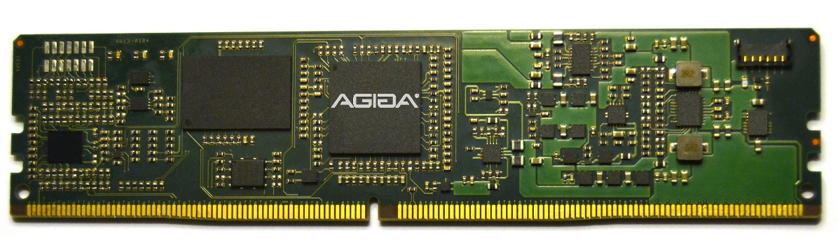
AgigA's DDR4 NVDIMM: A Future 3D XPoint Form Factor?
While Intel will clearly be pursuing the storage aspect of 3D XPoint through NVMe, I suspect Micron might take a more memory-like approach since it's a memory company as much as it's a storage company. It was made clear that 3D XPoint can be used in memory and storage applications because the technology is bit-addressible and can work in a similar fashion as DRAM. Bringing 3D XPoint closer to the CPU and connecting it through a DDR4 interface would obviously yield the best performance and eliminate any bottlenecks that PCIe has. There are already NAND-based products that do this, such as SanDisk's ULLtraDIMM, and a couple of months ago JEDEC paved the way by releasing a standard for DDR4 NVDIMMs, a new standard set to fill the gap between DRAM and SSDs. While NVDIMMs will require driver work due to the lack of standardized software interface like NVMe, I do believe 3D XPoint is the right technology for bringing NVDIMMs to the market and it would make sense for Micron to do so.
Applications
Section by Ryan Smith
The use cases for 3D XPoint are potentially significant in number and Intel/Micron believe that it will open the doors for all sorts of new applications. Overall the computing industry has had access to high speed non-volatile memory technologies before – magnetic core memory is the traditional poster child here – so there is some precedence here and some fundamental research into the field from the early days of computing. However with magnetic core memory having become outmoded before the majority of our readers were even born, the modern computing industry has developed around the current paradigm of fast DRAM and slow permanent storage. As a result while the potential applications are numerous, it’s still in many ways an uncharted area in computer science.
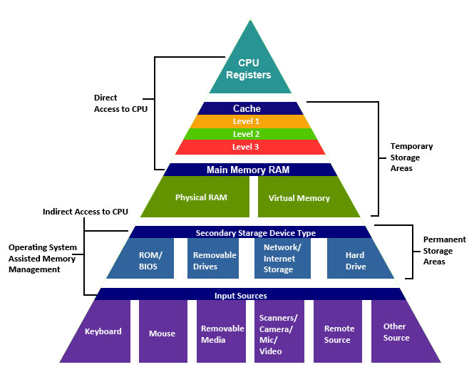
The most immediate application of 3D XPoint based products will be as a layer of storage between DRAM and SSDs. Over the history of computing the number of layers between storage and processors has continued to build – multiple layers of on-die caches, off-die caches, caching SSDs, etc – and 3D XPoint memory would further fit into that heiarchy as a storage medium that bridges the gap between DRAM and the current fastest non-volatile storage. By treating 3D XPoint memory as another layer of cache, 3D XPoint can be used to further speed up applications that are currently bound by either memory capacity or storage latency.
 <
<
The Traditional Memory Heiarchy (Image Source: Tommy MacWilliam, Harvard)
Given the costs of 3D XPoint, the first such applications are expected to be on the enterprise side. Enterprise users make heavy use of storage at all layers in order to balance performance needs against the relatively small capacity of DRAM. Database servers in particular adapt well to caching, and it’s easy enough to imagine a next-generation database system using 3D XPoint to backstop DRAM. Since 3D XPoint is non-volatile, it can even be an exclusive cache – that is, its contents don’t need to be in lower layers as well – which eliminates a good deal of overhead. A database system in this context would only need to write contents to SSDs and other, lower layers of storage when data gets expelled from the 3D XPoint cache, an occurrence that may be particularly rare with the properly tuned database.
Many of these benefits of a cache layer are applicable to other types of storage-heavy servers as well, though I expect databases will be the king. Perhaps the more interesting aspect – and certainly more relatable to the public at large – will be what 3D XPoint-backed servers are used for. Intel and Micron are eager to point out the “big science” uses for the technology; projects and systems such as the Large Hadron Collider and Oak Ridge’s Titan supercomputer can generate a massive amount of data, and while processing all of that data is first and foremost a processor issue, feeding that data for processing is a big problem as well. Any kind of analysis that could benefit from individual processors having RAM-like access to an SSD-sized pool of data could benefit.
The catch is that there’s still a lot of research that’s needed into figuring out what the best uses may be. This kind of shift in access times and capacity doesn’t just make computers faster, but it can change the fundamentals of what algorithms are best. Just as how GPUs required scientists to figure out how to spread out their work in a massively parallel (and high latency) nature, putting 3D XPoint to its full use will require newer algorithms that are capable of effectively utilizing direct access to so much data at once.
Meanwhile I would be surprised if the financial industry didn’t jump on this early, as they are prone to jumping on major technologies in order to try to get an edge in a highly competitive and lucrative field. In this aspect it’s not so much that 3D XPoint would improve processing speed – such work is already offloaded to large RAM pools when possible – but rather it would enable traders and analysts to run simulations against much larger datasets much more effectively.
As for the consumer space, the same principles about an additional cache layer would apply, but I’m not so sure we’d see consumers pick it up in the same manner. Much of this has to do with what the eventual costs and capacities of 3D XPoint products would be, as consumers are much more price sensitive than professional users. In the consumer space we’ve seen sporadic use of NAND-backed hard drives, for example, but by and large consumers have stuck with discrete SSDs and HDDs. Consumers either don’t want to pay the premium for SSDs, or have enough money to just buy large SSDs outright, leaving little of a middle ground.

That said I’ve seen some interesting pitches for 3D XPoint in the gaming space that have some merit, as games are something of a special case for consumer workloads. By and large we want fast access to game resources since those resources are accessed on-demand and are needed to progress in a game’s execution, but the assets themselves aren’t volatile. Only a small part of the working set for a game is volatile data – player positions, AI decision trees, game state, etc – while the rest of it is static data such as models, world geometry, and textures. 3D XPoint in turn would be fast enough that it could be used as a replacement for RAM in holding these assets, but as the data is non-volatile it wouldn’t thrash 3D XPoint P/E cycles very much, and any write speed disadvantage compared to DRAM would be immaterial.
But again, this is going to depend on the cost of the technology; if it were to become cheap enough that 50-100GB could be thrown in a game console or gaming PC, then you could store the entirety of most games in 3D XPoint memory, which would reduce load times to the time required to process the data and setup the game state. This is more important in consoles which currently store their games on a mechanical drive, who then could recall data rather quickly on first boot or adjust for large amounts of memory swapping for more detailed titles. High end PCs with large amounds of DRAM can already use RAMDisks perhaps nullifying a point there.
Last but not least of course are the implications for 3D XPoint as a wholesale replacement for DRAM. The more limited lifetime of 3D XPoint relative to DRAM certainly poses some challenges in this respect, but I suspect the bigger issue will be overall bandwidth. By the time 3D XPoint becomes available in bulk, DRAM technology should be to the point where faster-generations of DDR4 are available and HBM is widely deployed. Given that future generations of HBM are targeting 1TB/sec or more of memory bandwidth, it’s unlikely that 3D XPoint is going to be able to match the bandwidth of contemporary high-bandwidth DRAM solutions. So any rumors of the impending death of DRAM are likely premature.
IoT & Embedded, A Good Fit For 3D XPoint?
But with that said, while 3D XPoint isn’t likely to replace DRAM in a wholesale manner for all applications, there is clearly room for it to replace DRAM in some situations where DRAM is used primarily for its bandwidth and latency versus solid state storage. Replacing DRAM with 3D XPoint in embedded applications for example would be very practical – many embedded uses don’t need high bandwidth or low latency as much as they just something better than traditional NAND – and I wouldn’t rule out smartphones here either, at least to an extent. If individual 3D XPoint chips can be produced small and cheap enough, then the most lucrative use for the tech as a DRAM replacement may be in the vast legions of low-performance devices, rather than in high-performance hardware that actually needs the full speed and latency of DRAM.


80 Comments
View All Comments
Pork@III - Friday, July 31, 2015 - link
1000X1000X10=3 Touch my crazy math! "Analyze This"Wwhat - Saturday, August 8, 2015 - link
Didn't intel slides on future CPU's talk about the new RAM? That would mean they might create their own market and there is no need to hope someone is interested really, if it's architecturally a (semi-)requirement for intel based systems.Wwhat - Saturday, August 8, 2015 - link
Oh excuse me, wasn't meant to be a reply but a standalone comment.Russ.Dill@gmail.com - Friday, July 31, 2015 - link
I was really excited about this article due to the leadup on Twitter. But I'm really disappointed on the coverage of the technology.I think Ian has a bit of confirmation bias going into this and did not examine PCM closely enough:
> During the discussions after the announcement, we were told
> categorically that this is not a phase change material, eliminating
> one potential avenue that it might be the change in the crystal
> structure of the cell producing the resistance change.
Here's the portion of the webcast:
https://www.youtube.com/watch?v=VsioS35D-HY&t=...
"So…so let me take the first piece while Rob you jump in. First…first of all you shouldn't think of this as NAND or DRAM. You should think of it as a whole new class of memory. It…it…it…it really does fill it's own unique spot. Now it can be used in more of a storage type of application or it can be used more as a system main memory and we think it will be used as both. Uh…uh f…for different applications and different reasons. Um, but it really kinda fits in that…in that unique spot.
Now rel…I'm not familiar with sigma RAM I'm sorry maybe…maybe Rob is, but…but relative to…to phase change which has been the market before and which Micron has some experience with in the past. Uh, again, this is uh, this is a, this is a…a very different architecture in terms of the place it fills in the…in the…in the memory hierarchy because it has these…these dramatic improvements, uh, in speed, uh, and…and volatility and, uh, performance."
I don't view that as a categorical denial that it's PCM. Just that it's a different architecture than the PCM product had out before, which it is. This is cross point. And there is a lot of hesitation in this response and it seems like rather than trying to answer the technology question, he goes back on message.
Along with patents, linkedin profiles (Employee confirms working on a 2xnm PCM 3D cross-point chip since January 2014, see Giulio Albini), and the mentions in the webcast of "property change" and "bulk material".
Russ.Dill@gmail.com - Friday, July 31, 2015 - link
The interesting thing is that 2xnm PCM cross point technology has been on the roadmap for a while, but in 2014, mention of PCM was phased out. The 2014/2015 materials still mention "other technologies" though. It could be that the technology failed. It seems more likely that there is some legal or corporate strategy for not mentioning the technology.2013 Fall and Summer slides: http://i.imgur.com/pAHeUPH.png
Ian Cutress - Friday, July 31, 2015 - link
We had a separate question and answer session with Greg Matson, SSD Director at Intel. When specifically asked if it was PCM, he said he could confirm that it was not.Russ.Dill@gmail.com - Friday, July 31, 2015 - link
I'm guessing this Q/A session was not recorded, can you give an actual quote? Are they just arguing semantics and claiming that it is PCMS?Ian Cutress - Friday, July 31, 2015 - link
OK now that I'm at a computer I can respond properly.Kristian attended the event live, I was at the UK briefing led by Greg Matson, so all questions on my end went through him with other press based in the UK, so no it was not recorded. It was specifically asked 'Is this Phase Change?' and he responded 'I can confirm it is not Phase Change'. The other journalist at that Q&A that I've seen pick up on this was the one that asked the question, Chris Mellor from The Register. Check his tweets on the subject as a double confirmation:
https://twitter.com/Chris_Mellor/status/6267342455...
https://twitter.com/Chris_Mellor/status/6267347543...
If you read through Chris' piece on XPoint, he comes to similar conclusions based that a 64Mb phase change demo with an ovonic switch last year was different to Micron's slide demonstration of XPoint with a diode-based selector.
So standard PCM/PCMS revolves around bulk crystal structure changes and metastable forms to differentiate resistive states, hence the 'phase' part of phase change. Arguably conductive bridging is also a change in phase, from a charged ion to a conducting metal, although is not specifically called phase change as such. It could also not necessarily be called a 'bulk change' as mentioned by Intel, although if the electrolyte layer is thin it would certainly act like bulk between the electrodes.
PCM, as of last year, was also considered one of the front runners leading into the technology based on information released although there have been reservations based on the currentneeded to transition current materials and the respective heat. Given Micron's investor briefing slides, conductive bridging is still perhaps the most likely, especially given how Matson answered the PCM question with an affirmative no. I understand that a few analysts have stated is PCM, given the watchful eye on patents and so forth, but coming direct from the source is hard to ignore with all the other suggestions.
As Kristian points out, Micron's investor roadmap points to a second technology in a couple of years also entering the market. If this isn't PCM, that could be, or vice versa. Or even STT.
Just for the record I'm merely trying to pinpoint where the evidence leads me, rather than introduce any sort of bias here. Without a direct SEM or quote from Intel, we can't be sure. Both PCM and CB can be done with many different materials, and I'd hazard a guess there are combinations that haven't been made public. So we're still talking about general methodology rather than specific physical interations between named structures.
If anyone comes up with anything else, I'd be glad to hear and read it.
Russ.Dill@gmail.com - Friday, July 31, 2015 - link
They have two future memory tech on their timeline, A and B. Perhaps we are seeing A now, and B is phase change.Russ.Dill@gmail.com - Friday, July 31, 2015 - link
BTW, I am still leaning very strongly towards PCM. It of course seems unlikely in the highest degree that Matson could of misspoken on something so basic. Maybe I'm not familiar enough with the tech industry, but it seems so very strange that they are so cagey on the tech. There must be a very strongly company wide memo from legal. They seem to be able to confirm that it is a resistive memory element, but nothing beyond that. So from that aspect, it seems strange that someone would be willing to go on record stating what type of resistive memory element it is not.Given the number of companies with promising cross point style resistive memory architectures (many of them PCM, eg, ST), and the patent warchests to go with them, there is likely to be a legal battle that will make the whole RAMBUS thing seem like it was a small claims case.
I wonder what event is gating release of tech details. Is it a legal agreement? A patent date? A pending legal action?