The Surface 3 Review
by Brett Howse on May 4, 2015 9:00 AM ESTPowering the Surface 3: Intel’s Atom x7 System on a Chip
I still remember when back in 2011 Intel announced that they were finally going to stop treating Atom as a second class citizen at the manufacturing level, and bring it in line with the company’s mainstream Core processors. After having drawn out the 45nm and 32nm Atoms for too long, and suffering in the marketplace versus ARM as a result – Intel realized that to combat the growing threat of ARM they would need to treat the mobile market more seriously, and they would need to commit their sizable manufacturing advantage to the field to do this.
Now even Intel can’t turn on a dime – processors design begins half a decade in advance these days – so what have seen is a gradual ramping up towards this point. Silvermont, Intel’s first 22nm Atom, would introduce a more modern and better performing out-of-order architecture for Atom, meanwhile Intel would catch up on the manufacturing side by not producing 2 generations of Atoms on the 22nm node. Instead Silvermont would be the only 22nm Atom, and was to be followed by 14nm Airmont roughly a year later.
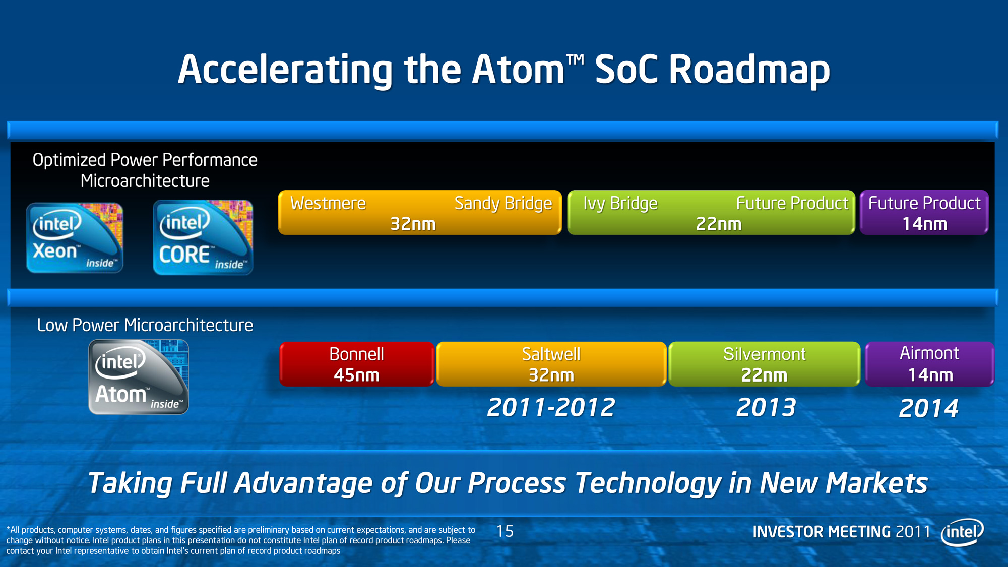
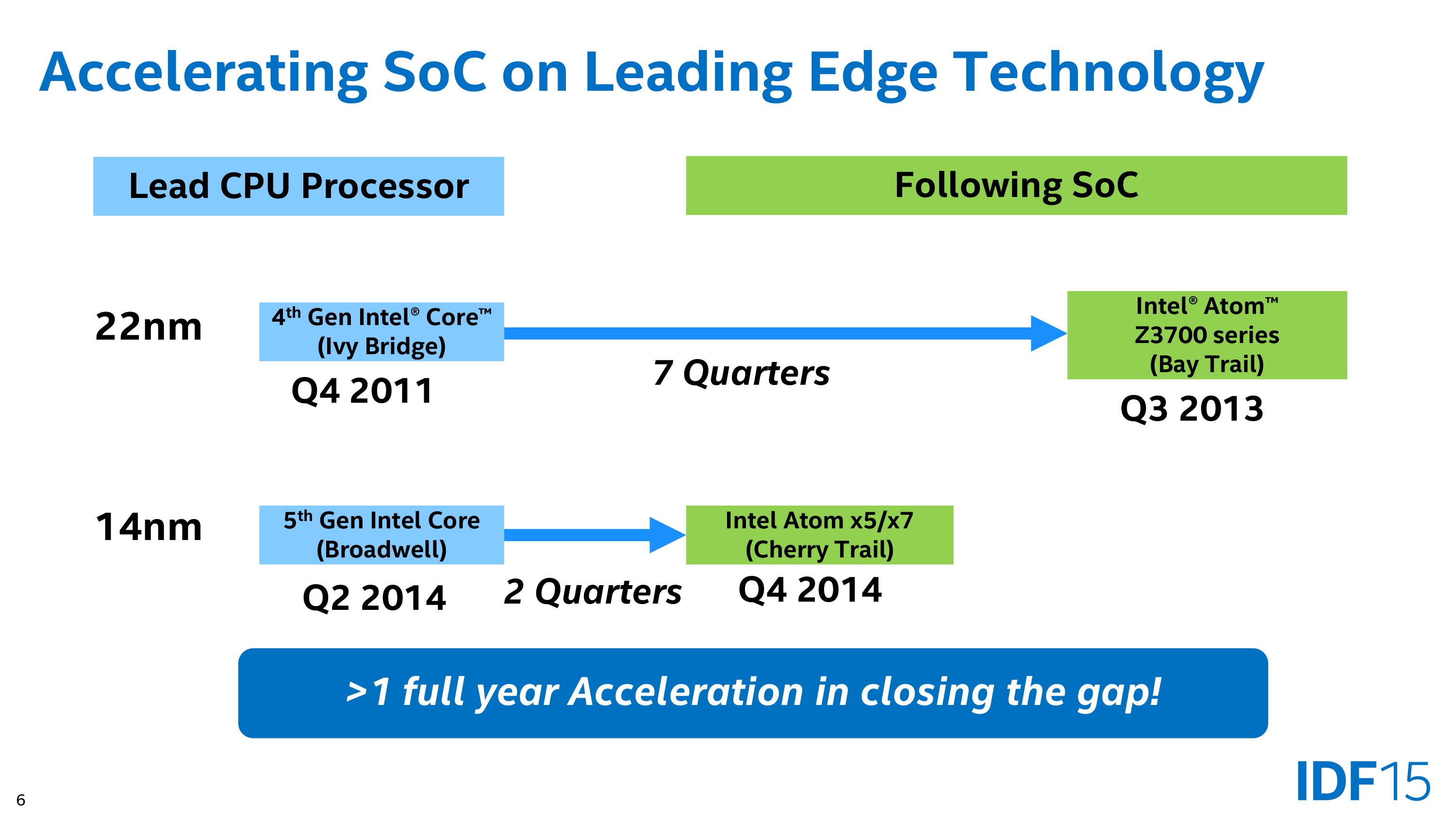
With Intel’s initial 14nm problems that year later ended up being a bit longer than a year, but in 2015 we’re finally there, and the change is remarkable. Only one generation ago, Intel launched their 22nm process as they always do, with desktop and high-performance laptop processors first. Now with 14nm the tables have been turned; Atom didn’t get first-dibs on 14nm – that went to Core M – but Airmont is still going to beat Intel’s desktop and high-performance Broadwell SKUs to the retail market. In one generation Intel has gone from favoring the desktop to favoring mobile, that’s how serious Intel has become.
That brings us to Surface 3, and the SoC powering it: Cherry Trail. The successor to the Silvermont-based Bay Trail that has powered so many x86 tablets in the last year, Cherry Trail is a distinct tick in Intel's tick-tock cadence. What this means is that Intel has largely retained the same architecture as in Bay Trail, investing in a fairly small number of updates, looking to take advantage of the power consumption and die size (cost) benefits of 14nm. To that end Intel has not even bothered to announce any major architectural changes for Airmont, and while there will likely be a few tweaks made to the CPU to make it work more efficiently on 14 nm, we will have to wait for Goldmont for the next big Atom architecture.
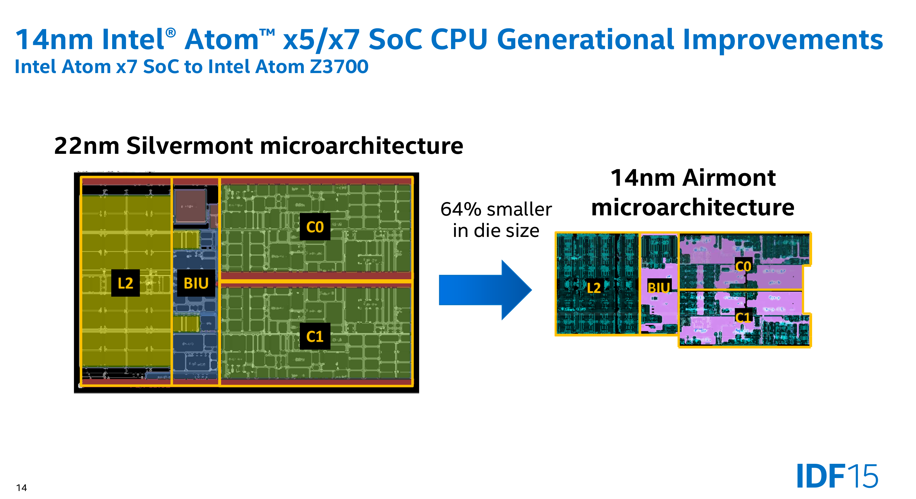
Cherry Trail itself is a fairly small chip. While Intel hasn’t released an official die size for it (no more than they did Bay Trail), from various IDF presentations they have released official numbers for the complete package, and decent photos as well. As a result we can take a decent stab at die sizes, and from Intel’s photos we’d estimate that the die size is around 83mm2. Unfortunately we don’t have anything quite comparable to Bay Trail, though we believe it to be a good bit smaller than Intel’s previous generation tablet SoC. At 83mm2 this would put the die size at quite a bit smaller than Apple’s A8X tablet SoC, and actually is just a hair smaller than the A8 phone SoC’s 89mm2.
Diving a bit deeper, Intel has also released some size data for individual Silvermont/Airmont CPU modules. The dual core modules, which contain the 2 CPU cores along with L2 cache and appropriate glue, have shrunk significantly from Silvermont to Airmont. Overall the Airmont CPU module is 64% smaller than the Silvermont module. And to be clear that does not mean Airmont is 64% of the size of Silvermont, that means that Airmont has been reduced by 64%; relative to Silvermont it is only 36% of the die size. Intel has achieved a better scaling factor than 22nm to 14nm alone, indicating that they have almost certainly enacted further optimizations to bring down the die size as an architectural level.
Moving on to the architecture of Cherry Trail, each Airmont core is a two-wide instruction decode with out of order execution. The L1 cache is 32 KB 8-way associative for instructions, and 24 KB 6-way associative data cache. Level 2 cache is 16-way associative with 1 MB of cache shared between two cores. There will be either two or four core versions available, which means that each SoC will have between 1 and 2 MB of L2 cache depending on the number of cores. There is no L3 cache on Atom.
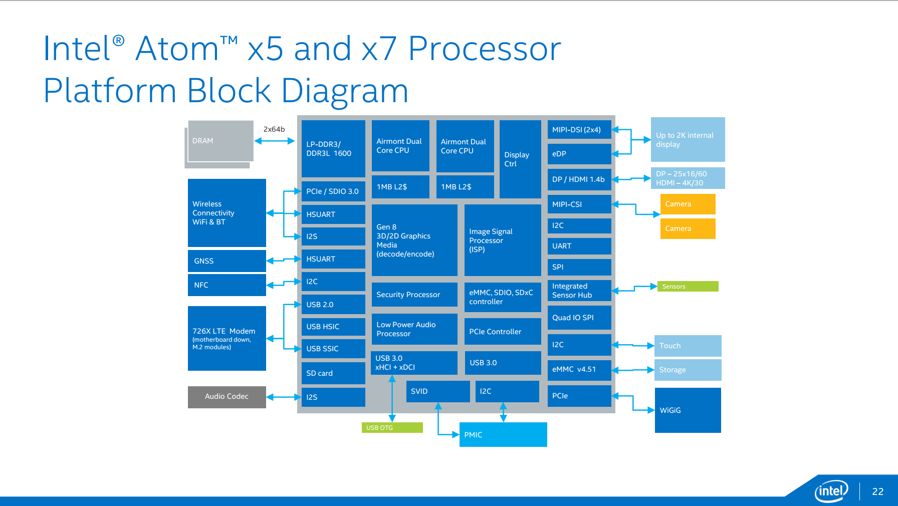
The System on a Chip (SoC) has support for LP-DDR3 or DDR3L 1600 in dual-channel configuration, and has the blocks needed for PCIe 3.0, USB 2.0, USB 3.0, and support for up to three displays with eDP, DP, and HDMI 1.4b. The built in storage support is eMMC v4.5.1, which is typical for a tablet class processor.
Here is a Block Diagram of the SoC.
The one truely major change to the SoC is the inclusion of Intel's Gen 8 Graphics. Bay Trail used Gen 7 Graphics from Ivy Bridge, and Bay Trail only had 4 Execution Units (EUs) available. Cherry Trail ramps that up significantly, with the latest Gen 8 Graphics from Broadwell now onboard, bringing forward Intel's GPU enhancements over the last two half generations, not to mention the compute enhancements as well.
In terms of execution hardware the x7-8700 model has 16 EUs available, indicating that Intel has spent a significant amount of their die size savings from the 14nm process on graphics resources. Gen 8 has eight EUs per sub-slice but a minimum of three sub-slices in the design, and therefore in order to improve SoC yields the thread scheduler will dynamically allocate the right amount of cores per-subslice to total 16. For comparison, Intel's Broadwell line of Core processors have a minimum of 23 (but most have 24) EUs available, and a maximum of 48, so with Cherry Trail Intel has closed the top-to-top gap in execution resources between Core and Atom to just 3-1.
In Intel’s datasheets, the Atom GPU is labeled as Gen8-LP to designate that this is a low power model being used in a tablet. The base frequency for this GPU is 200 MHz, with a boost of 600 MHz.
In addition to the GPU update, the ISP and hardware decode capabilities get a bump as well. There is full hardware acceleration for decode of H.263, MPEG4, H.264, H.265 (HEVC), VP8, VP9, MVC, MPEG2, VC1, and JPEG, as well as hardware encode for H.264, H.263, VP8, MVC, and JPEG. This marks the first Intel product to ship with the company's full, fixed-function HEVC decoder, making Atom the company's most advanced media processor, at least for this short moment.
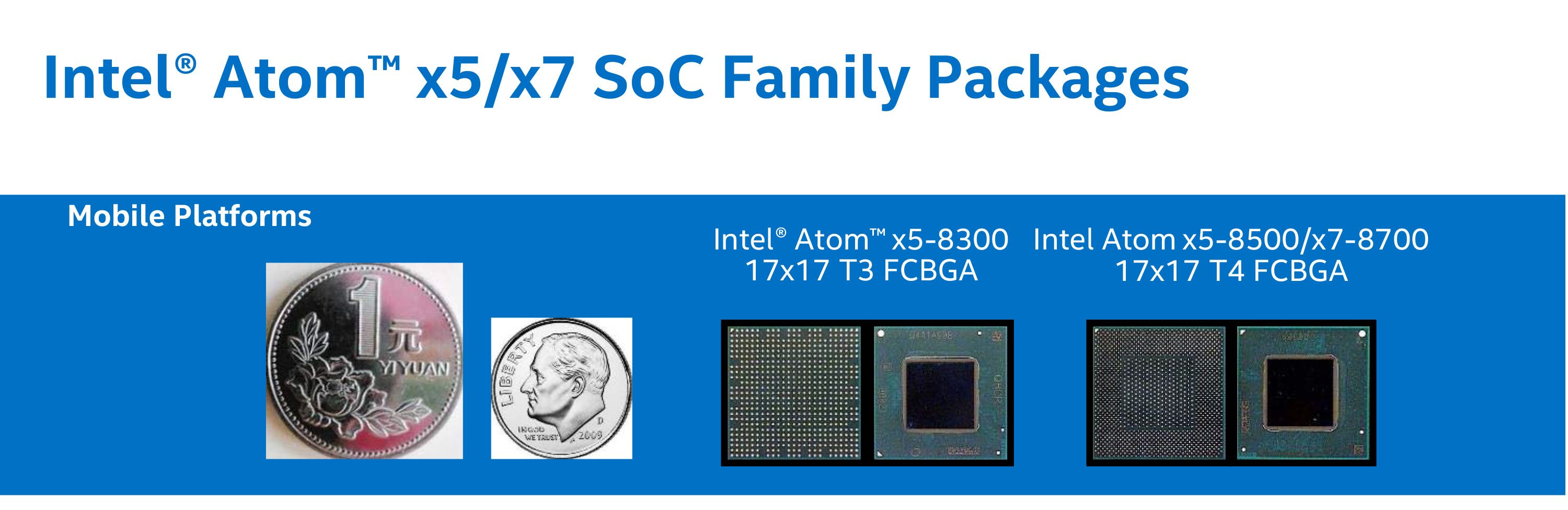
The overall SoC is 17mm x 17mm, and the Z-height is 0.937mm, so it is quite a bit smaller than Core M’s 30mm x 16.5mm x 1.05mm package. Intel is not listing a Thermal Design Power for the Atom chip, but is instead listing it as a Scenario Design Power of 2 watts. The CPU base frequency is 1.6 GHz with a turbo frequency of 2.4 GHz, and there is also support for a Low Frequency Mode of just 480 MHz for extra power savings when needed.
| Atom x7-8700 | Atom Z3785 | |
| Architecture | Cherry Trail (Airmont) | Bay Trail (Silvermont) |
| Cores / Threads | 4 / 4 | 4 / 4 |
| Base Frequency (MHz) | 1.6GHz | 1.5GHz |
| Turbo / Burst (MHz) | 2.4GHz | 2.4GHz |
| L2 Cache | 2 MB | 2 MB |
| SDP | 2 W | 2.2 W |
| GPU Architecture | Gen 8 | Gen 7 |
| GPU Execution Units | 16 | 4 |
| GPU Frequency / MHz | 200-600MHz | 313-833Mhz |
| DRAM | LPDDR3-1600 | LPDDR3-1333 |
So what we really have here is a massaged Bay Trail class chip, but the 14 nm process should allow for a higher period of sustained turbo frequencies to help out with performance. It will be interesting to see what Intel does with Goldmont, and if they will add things like hyper-threading or not, but that discussion is for another time.


265 Comments
View All Comments
Brett Howse - Tuesday, May 5, 2015 - link
Windows Video app is used, and the file properties are listed on the graph. Let me know if you need anything else.MarcSP - Thursday, May 7, 2015 - link
No, that will be all. Dismised. :PHe, he. Thank for your reply! :-)
dusk007 - Monday, May 4, 2015 - link
One would wish Intel would just license the Mali GPUs or PowerVR designs. Even with 14nm they cannot keep up with Nvidia, Apple or any of the faster Adreno or Mali 760 SoCs.Also there doesn't seem to be any improvements. Their GPU design is not very power efficient and seemingly not even die space efficient but there are no real noticeable improvements between Gen 7 and 8. They should just go back to licensing or just buy Imagination Technologies.
Drumsticks - Monday, May 4, 2015 - link
Correct me if I'm wrong but don't skylake rumors include huge GPU strides?A5 - Monday, May 4, 2015 - link
Big grain of salt on that. Similar rumors were around for Haswell and Broadwell, too.lilmoe - Monday, May 4, 2015 - link
You'd think they'd at least get the GPU at performance parity with AMD's APUs by now....meacupla - Monday, May 4, 2015 - link
I think intel GPU performance is better than AMD APUs. Intel's solution does hardware video playback without sucking down enormous amounts of power.I won't even go into gaming, since both solutions are, flat out, subpar for that.
anubis44 - Monday, May 4, 2015 - link
Utterly wrong. AMD's Radeon GPU technology in their APUs crushes Intel's fastest integrated graphics. No comparison. Don't even try.meacupla - Tuesday, May 5, 2015 - link
That's not what I'm saying. Please read.AMD is faster, but at the cost of power and efficiency. And it still won't give you a good gaming experience, because there's not enough of everything in APUs.
Intel is slower, but gets the job done with regards to video, there was no question of it being gaming capable in the first place.
lilmoe - Tuesday, May 5, 2015 - link
Efficiency isn't AMD's fault. Intel's had the process lead for more than 2 generations now and they're STILL not even close to AMD's GPU performance... We'll see how efficient Intel's GPU is when AMD goes 14nm....