GeForce GTX 970: Correcting The Specs & Exploring Memory Allocation
by Ryan Smith on January 26, 2015 1:00 PM ESTDiving Deeper: The Maxwell 2 Memory Crossbar & ROP Partitions
Now that we have a basic understanding of the proper specifications of the GTX 970 we can dig deeper into its architecture and layout. As we mentioned previously, the GTX 970 ships with an unusual configuration, one we’ve never quite seen before. In it, thanks to a new feature of the Maxwell architecture, NVIDIA has been able to disable part of a ROP/Memory Controller partition, something that they could not do on Kepler or earlier generation designs. As a result of this the intended behavior of the GTX 970 is different than the GTX 980 or any theoretical Maxwell part with a completely disabled ROP/MC partition.
The biggest impact of this configuration is that it creates the segmented memory conditions NVIDIA outlined in their earlier statement. Due to performance issues from the unbalanced ROP/MC partition, NVIDIA segments the memory into a high-performance 3.5GB segment – what they refer to as segment 0 – and a low-performance 512MB (0.5GB) segment containing the rest of the RAM. It is this segmentation that results in some of the previously-unusual memory allocation behaviors and memory bandwidth benchmarks on the GTX 970.
But in order to understand just why the segments exist, how they are allocated, and how they influence performance, we first need to learn about the Maxwell memory crossbar.
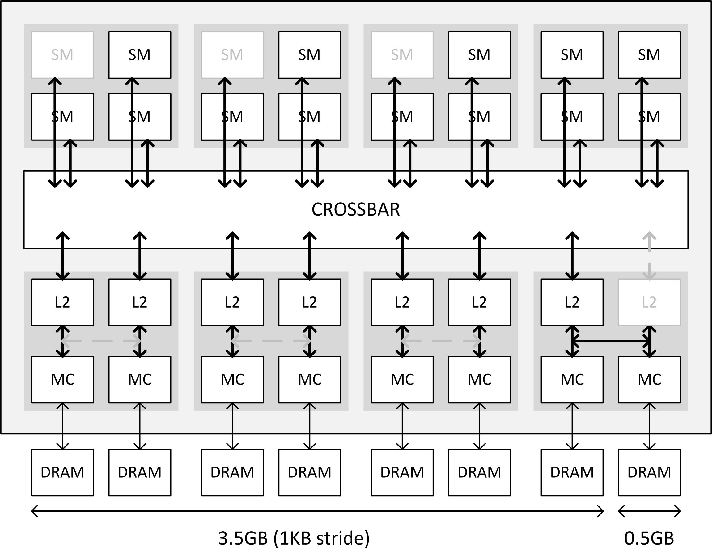
GTX 970 Memory Crossbar
In the above diagram from NVIDIA, NVIDIA illustrates at a high-level overview how the Maxwell memory crossbar is laid out, and specifically how it’s configured for GTX 970. In it we have the 16 GM204 SMMs at the top connected to the crossbar, meanwhile below we have 4 ROP/MC partitions, with each partition divided up into individual ROP/L2 units and memory controllers. Note that the specific units disabled on any GTX 970 chip will vary – it’s not necessarily the 1/3/5 SMMs or the last ROP/MC partition – but from a high level overview this is consistent for GTX 970 regardless of which specific physical units have been disabled.
In any case, while the crossbar shows how the SMMs and ROP/MC partitions are connected via the crossbar, memory segmentation is really a story about the ROP/MC partitions. The SMMs do not play a role in how GTX 970’s memory is configured – the crossbar abstracts all of that – and the crossbar itself matters only in as much as the ROP/MC partitions are connected to it.
When it comes to the ROP/MC partitions then, we can see first-hand in the GTX 970 what’s new in the architecture. In Kepler and previous generation designs, NVIDIA’s granularity for disabling ROP/MC partitions was all or nothing – either the entire partition was turned on or the entire partition was turned off. However starting with Maxwell, NVIDIA has gained the ability to disable the individual ROP/L2 units within a partition, allowing one of the two ROP/L2 units to be disabled. This essentially introduces a 3rd possible option: a partially-enabled ROP/MC partition, backed by two memory controllers and a single ROP/L2 unit. Meanwhile the memory controllers are still tied together, and disabling one of them requires disabling the entire partition.
| NVIDIA ROP/Memory Controller Configuration Options | |||
| Kepler | Maxwell | ||
| ROP/MC Partition Fully Enabled | ROP/MC Partition Fully Enabled | ||
| N/A | ROP/MC Partition Partially Disabled | ||
| ROP/MC Partition Fully Disabled | ROP/MC Partition Fully Disabled | ||
It’s this option that the GTX 970 leverages, and in doing so becomes the first Maxwell part to use this feature. NVIDIA has disabled 1 ROP/L2 unit, removing 8 “ROPs” (or rather 1 unit capable of 8 pixels/clock) and 256KB of L2 cache from the GTX 970. This is why the GTX 970 is left with 56 ROPs spread over the 4 partitions, along with 1.75MB of L2 cache.
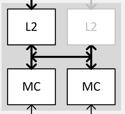
Meanwhile there’s one other new feature here that’s activated only on the partially disabled partition, and that’s the link between the first and second units of the ROP partition. Typically each ROP/L2 unit would have a link to a port on the crossbar and a link to its own dedicated 32-bit memory controller channel; however because GTX 970 disabled a ROP/L2 unit, the “buddy” link comes in to play. This link is essentially the lynchpin of Maxwell’s new partial disable functionality, and allows the second half of the memory controller to stay active. This link only needs to be active when a ROP/L2 unit is disabled, and NVIDIA has confirmed that it is a full bandwidth link identical to the normal ROP/L2 to MC link, meaning it’s capable of 4 32 byte requests per clock (2 reads and 2 writes). Ultimately this link is what makes a partially disabled partition possible, and is also what makes it possible to have the full 256-bit memory bus present and active in spite of the lack of a ROP/L2 unit and its associated crossbar port.
Finally, because of this configuration and the lack of a ROP/L2 unit we get to the memory segments. Although the full 256-bit memory bus is present and active on GTX 970 and capable of providing 224GB/sec of combined memory bandwidth between the DRAM modules and the memory controllers, it’s a bit of a misnomer to say the card has that much bandwidth between the memory controllers and everything else, at least in the same sense that the GTX 980 does.
Like virtually every other operation on a GPU, memory accesses are done in parallel to improve throughput. On a fully enabled card such as GTX 980 these operations are striped across all of the memory controllers in what NVIDIA calls a 1KB stride. In doing this, each and every 32 bit memory channel needs a direct link to the crossbar through its partner ROP/L2 unit. However in the case of the GTX 970 a wrench is thrown into the works, as there are 7 crossbar ports and 8 memory channels.
Ultimately due to the design of the crossbars and the memory controllers, it is not possible for 1 crossbar port to carry the full load of 2 memory channels in all circumstances. The crossbar port and its attached ROP/L2 unit can access both memory channels at once, splitting up the 4 operations among them, but there is only 1 read return bus and 1 write data bas, and hence in practice it cannot issue identical operations to both memory channels at once . As a result NVIDIA has segmented the GTX 970’s memory into the now-familiar 3.5GB and 512MB segments. In the case of the 3.5GB segment, this behaves otherwise identically to a fully enabled card such as the GTX 980, with the 1KB stride being striped over 7 crossbar ports, and hence 7 DRAM modules. Meanwhile the 8th and final DRAM module sits in its own 512MB segment, and must be addressed by the crossbar on its own.
This in turn is why the 224GB/sec memory bandwidth number for the GTX 970 is technically correct and yet still not entirely useful as we move past the memory controllers, as it is not possible to actually get that much bandwidth at once when doing a pure read or a pure write. In the case of pure reads for example, GTX 970 can read the 3.5GB segment at 196GB/sec (7GHz * 7 ports * 32-bits), or it can read the 512MB segment at 28GB/sec, but it cannot read from both at once; it is a true XOR situation. The same is also true for writes, as only one segment can be written to at a time.
Unfortunately what this means is that accessing the weaker 512MB segment blocks access to the stronger 3.5GB segment if both memory operations are identical; or put another way, using the 512MB segment can harm the performance of the 3.5GB segment. For example, if we want to issue reads to both segments at once, reading the 512MB segment blocks any other reads to the 3.5GB segment for that cycle. If the 3.5GB segment is blocked in this fashion and doesn't have a non-blocking write to work on instead, it would have to go idle for that cycle, which would reduce the effective memory bandwidth of the 3.5GB segment. This means that taken over time in our example, the larger the percentage of the time the crossbar is reading the 512MB segment, the lower the effective read memory bandwidth would be from the 3.5GB segment.
Despite all of this, achieving peak memory bandwidth performance on the GTX 970 is still possible, but it requires much more effort since simple striping will not do the trick. The easiest and most effective solution in this regard is to interleave reads and writes over the segments, such that one segment is writing while another segment is reading. Interleaving in this fashion allows both segments to work at once – avoiding the blocking effect of the shared read and write buses – and makes it more likely that both segments are doing useful work rather than waiting for their turn on an operation. However because this is only applicable to situations where more than 3.5GB of VRAM is in use and both segments are necessary, this means it's only theoretically possible to achieve 224GB/sec when more than 3.5GB of VRAM is in use. In any situations below 3.5GB we are de-facto limited to just the larger segment, in which case there are only 7 memory channels (196GB/sec) to stripe memory operations across. NVIDIA could of course interleave operations sooner than that and use both segments more often, but due to the blocking effect we've discussed before the performance hit from using the 512MB segment can quickly become greater than any gains.
The end result of all of this is that the GTX 970 has a unique memory layout that needs to be accounted for by the operating system and NVIDIA’s drivers, as the use of multiple segments adds a new level of complexity to optimizing memory performance. Unequal in size and performance, among the two segments the 3.5GB segment is a larger, faster, and otherwise more preferable segment to the 512MB segment. Which means from a logical hierarchical perspective, the 512MB segment essentially serves as an additional layer of memory between the main VRAM and system memory, being slower than the 3.5GB segment but offering almost 2x the performance of going out over the PCIe bus to system memory.
The upshot here is that while this is the first time NVIDIA has used this specific ROP/MC configuration in a product, this is not the first product they have designed with segmented or otherwise unbalanced memory configurations. Since the GTX 500 series, on some midrange SKUs NVIDIA has used unbalanced/asymmetrical memory configurations, most recently on the GTX 660 and GTX 660 Ti. In the case of both of those cards, NVIDIA utilized a 192-bit memory bus with 2GB of VRAM attached, which meant that some memory controllers had more VRAM attached to them than others. The end result as it turns out is very similar, and while NVIDIA has never explained in-depth how they handle memory allocation on those cards, it turns out that it’s very similar to GTX 970’s memory segmentation. Which is to say that NVIDIA actually has multiple generations of experience with segmented memory, and this is not the first time they have implemented it. Rather this is first time we’ve seen such a configuration on a high-performance card such as the GTX 970.
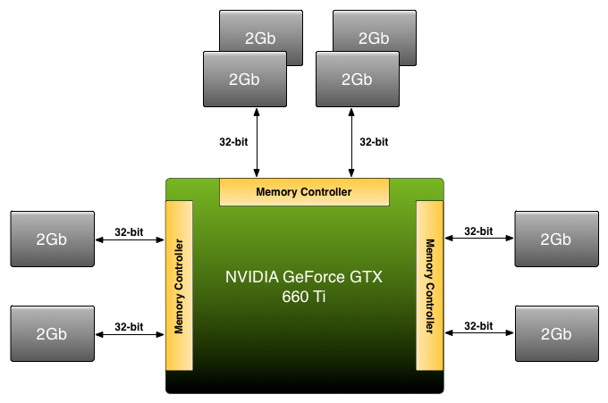
For Comparison: GTX 660 Ti's Unbalanced Memory Bus
| NVIDIA Maxwell Family Memory Controller Configurations | |||
| Part | Memory Segments | ||
| GTX 980 | 1 Segment (4x8 MC) | ||
| GTX 970 | 2 Segments (4x7 MC) | ||
| GTX 980M | 1 Segment (4x8 MC) | ||
| GTX 970M | 1 Segment (3x6 MC) | ||
| GTX 965M | 1 Segment (2x4 MC) | ||
As for why NVIDIA is using such a configuration here, the crux of the matter is money and yields. Without the ability to partially disable a ROP/MC partition, NVIDIA would either have to spec a card to use a fully enabled partition – essentially reducing yields for that card and driving up costs – or disable the entire partition and lose all of the benefits of the additional ROPs, memory, and the memory controller. This finer granularity allows NVIDIA to better control how they harvest bad chips and what resulting configurations they bring to market, along with making a single ROP/L2 defect less harmful to overall performance by keeping the rest of a partition online. Otherwise, to stick with a “balanced” configuration with as many crossbar ports as DRAM modules would result in either a higher spec GTX 970, or a lower spec card with a 192-bit memory bus.
In the grand scheme of things then, depending on how you want to define memory capacity the GTX 970 can be said to have either 3.5GB of VRAM or 4GB of VRAM. Only the first 3.5GB segment is a high-speed (full bandwidth) segment, and for naïve operations this is the segment that software will want to use. However the final 512MB segment is accessible, and despite its lower performance it is still usable and still far better than going to system memory, in which case GTX 970 has and can access a full 4GB of VRAM. This means that both answers can be correct, and like so many other facets of modern technology, the true answer is often more complex than a single number.


398 Comments
View All Comments
MrWhtie - Thursday, January 29, 2015 - link
"they set themselves up to hike prices in the future" hyperbole at its finest. Try again once you calm down and start speaking with some logic and reason.Casecutter - Wednesday, January 28, 2015 - link
^ It's simple they can't... They fused off one damaged defective L2 as they didn't have the volume of good GM204 to go to market with enough 970 parts. I would believe that the GTX 980M is a 12SMX part alought has all the L2 as the GTX980. They realy screw th pouch by touting "the GTX 970 ships with THE SAME MEMORY SUBSYSTEM AS OUR FLAGSHIP GEFORCE GTX 980".Nvidia came out and said "This team (PR) was unaware that with "Maxwell," you could segment components previously thought indivisible, or that you could "partial disable" components."
Had Nvidia called it 3.5Gb with Active Boost... or 4Gb Memory Compression... or something like that and explained I think a lot of folks would've taken interest and weigh that when making a choice... But we weren't privy to that information.
Elixer - Wednesday, January 28, 2015 - link
Looks like Nvidia is trying to make good.They will help you get a refund/credit for your 970 if you feel you want one.
http://forums.anandtech.com/showpost.php?p=3712051...
"I totally get why so many people are upset. We messed up some of the stats on the reviewer kit and we didn't properly explain the memory architecture. I realize a lot of you guys rely on product reviews to make purchase decisions and we let you down.
It sucks because we're really proud of this thing. The GTX970 is an amazing card and I genuinely believe it's the best card for the money that you can buy. We're working on a driver update that will tune what's allocated where in memory to further improve performance.
Having said that, I understand that this whole experience might have turned you off to the card. If you don't want the card anymore you should return it and get a refund or exchange. If you have any problems getting that done, let me know and I'll do my best to help."
MrWhtie - Wednesday, January 28, 2015 - link
Yeah right, they can't have my 970 back :P What am I going to buy instead, an AMD? (LOL!)CX71 - Wednesday, January 28, 2015 - link
> "What am I going to buy instead, an AMD? (LOL!)"That would be a good move ... TROLOLOLOLOL
mudz78 - Wednesday, January 28, 2015 - link
That's great news. Good see a company owning their mistakes and doing the right thing by consumers.The GTX 970 is still a good card, but purchasers have a right to make an informed decision before handing over their hard earned dollars.
Man_Of_Steele - Thursday, January 29, 2015 - link
If they really are accepting returns and refunds regardless of when you purchased your card, that would make this seem like it really was an honest mistake - despite the mistake seeming highly unlikely.As for me, 3.5gb VRAM isn't enough to justify $350-$400 (EVGA SC or SSC). I will wait and see what AMD does with the 390x, and wait and see if nVIDIA launches an 8gb (read 7gb) 970
Man_Of_Steele - Wednesday, January 28, 2015 - link
I understand that the cache isn't a huge issue, but as far as a future proof card, only 3.5gb VRAM..?You guys can form your own opinions, but that is a lot of people within the company that this error just so happened to slip past. There is also a notable stutter in Shadow of Mordor for those who haven't seen that yet.
What I am curious to see, is if there is a way to re-enable the ROPs and increase the clock on that last 500mb vram. This may be impossible and I'm just ignorant on the issue, but if someone knows please let me know if its possible!
MrWhtie - Thursday, January 29, 2015 - link
I don't think its possible, that last 500mb is slow because it only has one of its ROP/L2 units disabled (compared with 8 fully active on the 980). This causes one of the remaining ROP/L2 units to communicate with TWO of the 500mb DRAM sections (instead of 8 ROP/L2 each with their own 500mb DRAM.) Since it cannot access both 500mb secitions at once, it can only use 500mb in a "fast mode". When it tries to access both the speed is cut in half since normal operation is ONE ROP per 500mb DRAM. (The diagram on the second page illustrates this.)Its a hardware thing, its not a software issue whatsoever.
Man_Of_Steele - Thursday, January 29, 2015 - link
I saw the diagrams on a couple different sites, I just wasn't sure if they disabled it the smart way or the lazy way.Thanks for the clarification!