Intel Xeon E5 Version 3: Up to 18 Haswell EP Cores
by Johan De Gelas on September 8, 2014 12:30 PM ESTMemory Subsystem: Latency
To measure latency, we use the open source TinyMemBench benchmark. The source was compiled for x86 with gcc 4.8.2 and optimization was set to "-O2". The measurement is described well by the manual of TinyMemBench:
Average time is measured for random memory accesses in the buffers of different sizes. The larger the buffer, the more significant the relative contributions of TLB, L1/L2 cache misses, and DRAM accesses become. All the numbers represent extra time, which needs to be added to L1 cache latency (4 cycles).
We tested with dual random read, as we wanted to see how the memory system coped with multiple read requests. To keep the graph readeable we limited ourselves to the CPUs that were different. The Xeon E5-2695 and 2699 have a very similar memory subsytem (dual memory controller) so we tested only the E5-2699.
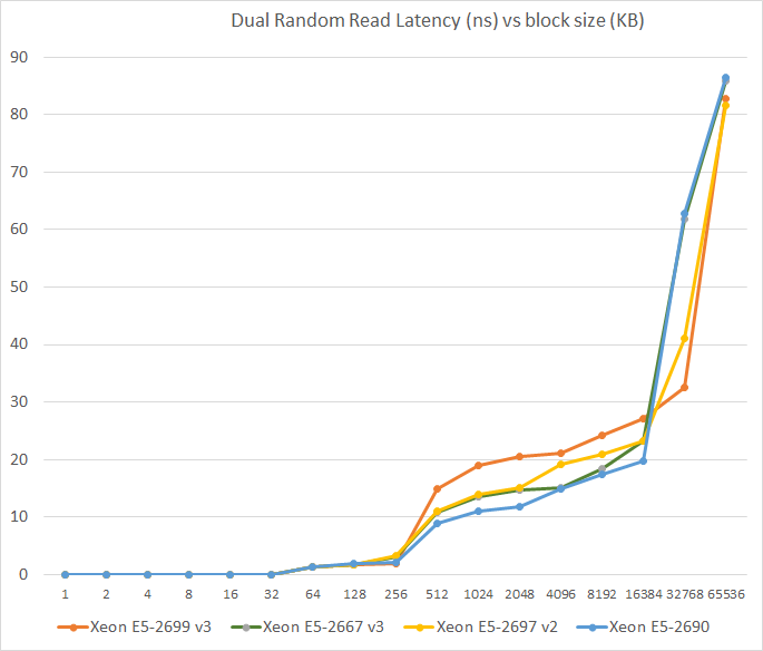
The massive L3 caches do have some disadvantages: latency goes up. The L3 cache of the Xeon E5-2699 v3 (45MB) has a latency between 20 and 32 ns while the 20MB cache of the Xeon E5-2690 hovers between 15 and 20 ns. That translates to about 90 cycles versus 60, which is considerable. However, it's not a case of the Haswell's L3 cache being a lot worse: the 20MB L3 cache of the Xeon E5-2667 v3 is only slightly slower than the Xeon E5-2690 and is still faster than the Xeon E5-2697 v2 (30MB). The main culprit is simply dealing with a huge amount of cache on the E5-2699 v3. In the next test, we will focus on the latency of the DRAM subsystem.
The DRAM subsystem is still three or four times slower than the massive L3 cache. LRDIMMs still have a very small latency overhead – +3.6% at the most – but that is neglible.
DDR4-2133 seems to have the same latency as DDR3-1866 . We measured 81.6 ns on the Xeon E5-2697 v2. Considering that DDR4-2400 is just around the corner, DDR4 will quickly give a performance boost to the new platform.


85 Comments
View All Comments
LostAlone - Saturday, September 20, 2014 - link
Given the difference in size between the two companies it's not really all that surprising though. Intel are ten times AMD's size, and I have to imagine that Intel's chip R&D department budget alone is bigger than the whole of AMD. And that is sad really, because I'm sure most of us were learning our computer science when AMD were setting the world on fire, so it's tough to see our young loves go off the rails. But Intel have the money to spend, and can pursue so many more potential avenues for improvement than AMD and that's what makes the difference.Kevin G - Monday, September 8, 2014 - link
I'm actually surprised they released the 18 core chip for the EP line. In the Ivy Bridge generation, it was the 15 core EX die that was harvested for the 12 core models. I was expecting the same thing here with the 14 core models, though more to do with power binning than raw yields.I guess with the recent TSX errata, Intel is just dumping all of the existing EX dies into the EP socket. That is a good means of clearing inventory of a notably buggy chip. When Haswell-EX formally launches, it'll be of a stepping with the TSX bug resolved.
SanX - Monday, September 8, 2014 - link
You have teased us with the claim that added FMA instructions have double floating point performance. Wow! Is this still possible to do that with FP which are already close to the limit approaching just one clock cycle? This was good review of integer related performance but please combine with Ian to continue with the FP one.JohanAnandtech - Monday, September 8, 2014 - link
Ian is working on his workstation oriented review of the latest XeonKevin G - Monday, September 8, 2014 - link
FMA is common place in many RISC architectures. The reason why we're just seeing it now on x86 is that until recently, the ISA only permitted two registers per operand.Improvements in this area maybe coming down the line even for legacy code. Intel's micro-op fusion has the potential to take an ordinary multiply and add and fuse them into one FMA operation internally. This type of optimization is something I'd like to see in a future architecture (Sky Lake?).
valarauca - Monday, September 8, 2014 - link
The Intel compiler suite I believe already convertsx *= y;
x += z;
into an FMA operation when confronted with them.
Kevin G - Monday, September 8, 2014 - link
That's with source that is going to be compiled. (And don't get me wrong, that's what a compiler should do!)Micro-op fusion works on existing binaries years old so there is no recompile necessary. However, micro-op fusion may not work in all situations depending on the actual instruction stream. (Hypothetically the fusion of a multiply and an add in an instruction stream may have to be adjacent to work but an ancient compiler could have slipped in some other instructions in between them to hide execution latencies as an optimization so it'd never work in that binary.)
DIYEyal - Monday, September 8, 2014 - link
Very interesting read.And I think I found a typo: page 5 (power optimization). It is well known that THE (not needed) Haswell HAS (is/ has been) optimized for low idle power.
vLsL2VnDmWjoTByaVLxb - Monday, September 8, 2014 - link
Colors or labeling for your HPC Power Consumption graph don't seem right.JohanAnandtech - Monday, September 8, 2014 - link
Fixed, thanks for pointing it out.