Intel Broadwell Architecture Preview: A Glimpse into Core M
by Ryan Smith on August 11, 2014 12:01 PM ESTPutting It All Together: Small Core M
Next to power constraints, the final element of Intel’s fanless challenge is the size of the SoC itself. Sub-10mm thickness doesn’t just put constraints on the heat capacity of the device but it also constrains just how large an SoC and its supporting circuitry can be. As a result Intel has focused on making Broadwell-Y the smallest Core processor yet, making the entire SoC under 500mm2 in size.
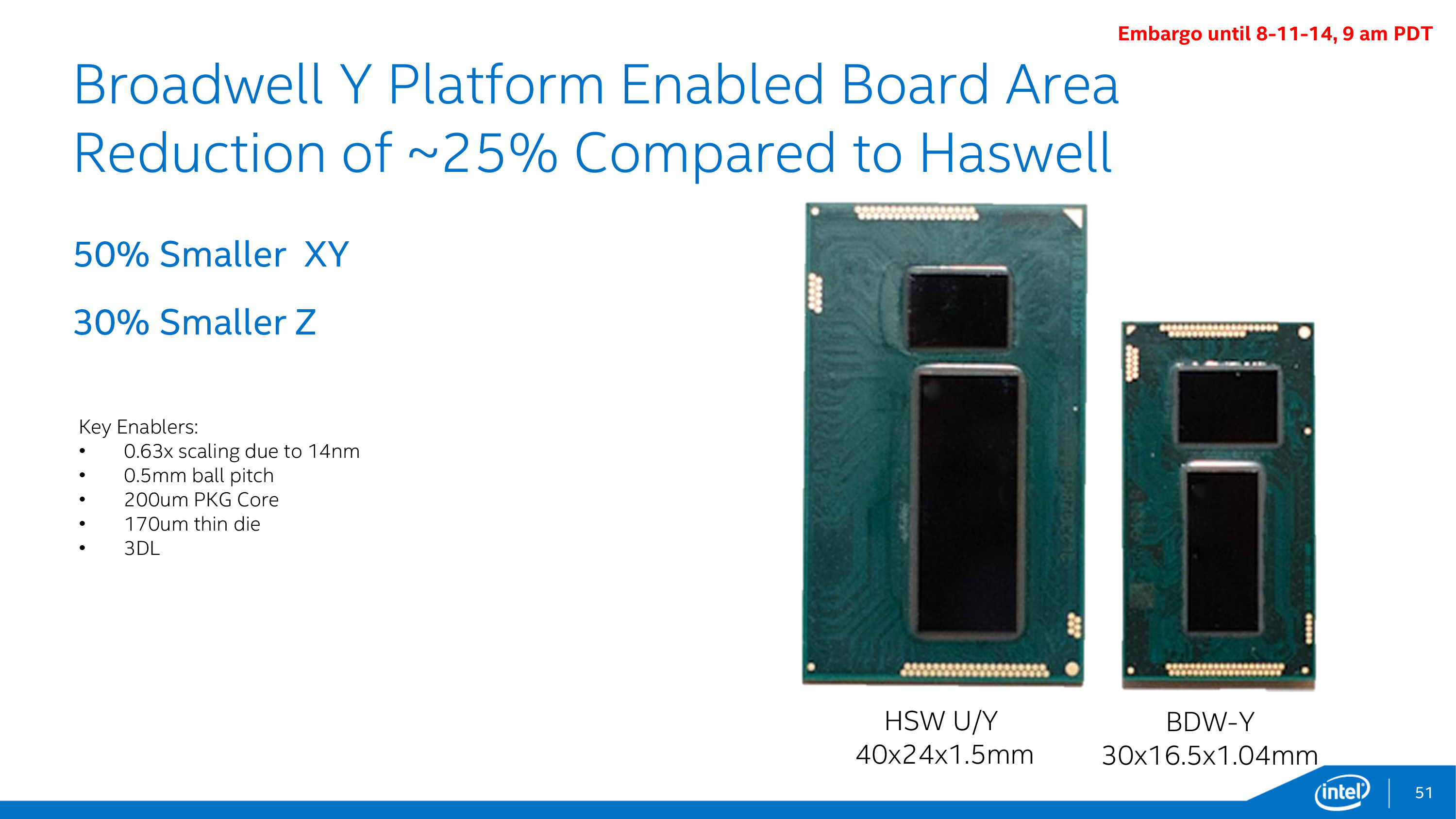
As was the case with power, reducing the size of Broadwell-Y is a multi-faceted effort. The 14nm process plays a big part here, allowing for one of the smallest Core CPU dice yet. At 82mm2 the Broadwell-Y CPU die is some 37% smaller than the Haswell-Y CPU die, none the less packing a dual-core CPU and a full GPU slice.
With such a small die Intel was in turn able to reduce the size of the entire SoC package through the combination of the reduced die area and further optimizations to the packaging itself. Haswell-Y’s already small ball pitch of .65mm was further reduced to just .5mm, producing a package with Intel’s smallest solder ball pads yet. Intel considers the reduction in the ball pitch to be the key change that allowed Broadwell-Y to be so small, as they were already pad-limited on Haswell-Y despite having ample excess packaging even after taking the CPU die’s larger size into account. As a result Broadwell-Y takes up almost 50% less surface area (XY) than Haswell-Y.
Intel has also made a number of changes for Broadwell-Y to reduce the Z-height of the Y SoCs, as even 1.5mm for the SoC starts to become a significant design constraint in a sub-10mm device. Again owing to the 14nm process, the Z-height of the Broadwell-Y die itself is down to 170um. Meanwhile the Z-height of the substrate has been cut in half from 400um to 200um, which accounts for nearly half of the total reduction in SoC Z-height.
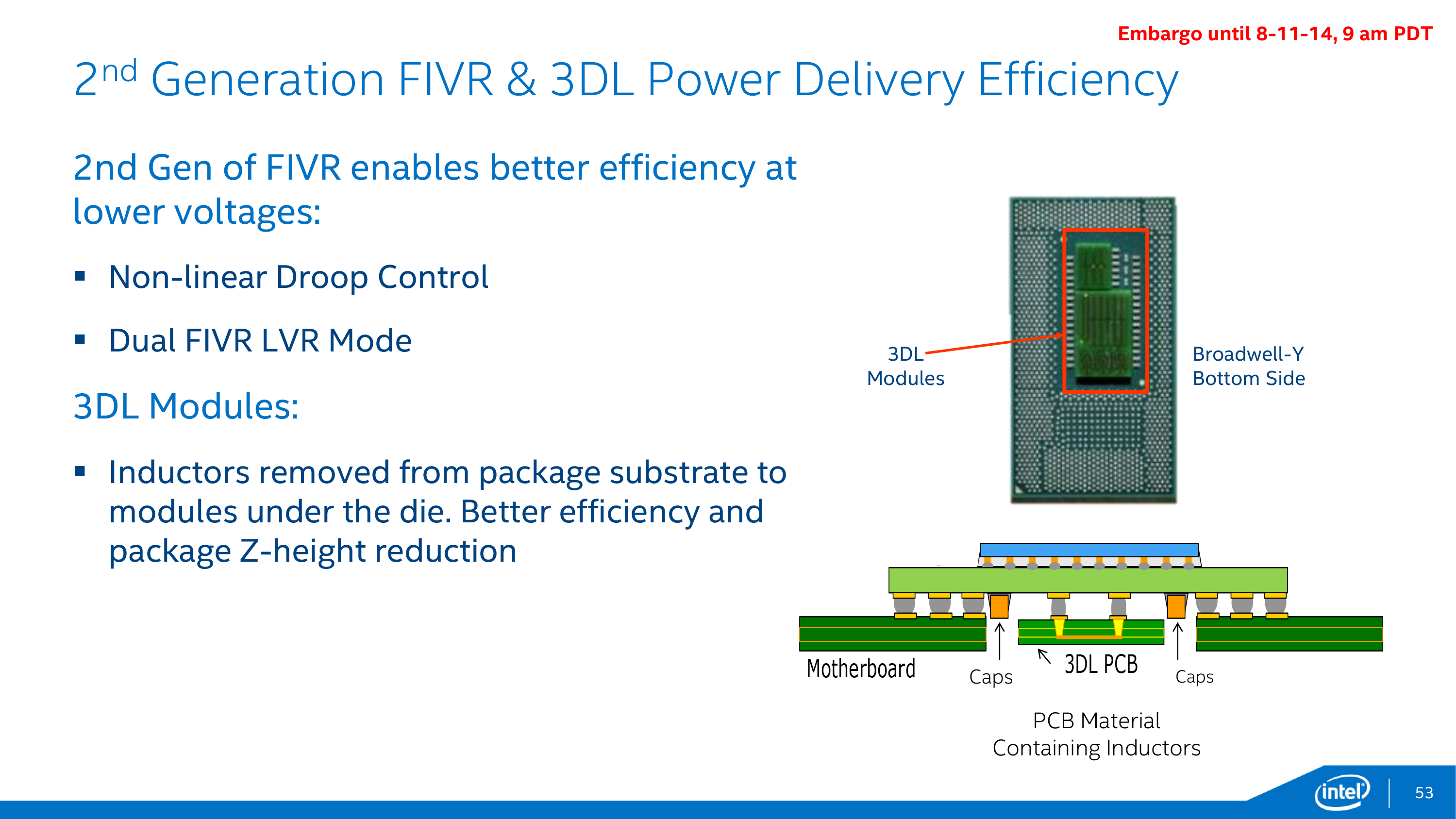
The final element in reducing the SoC Z-height, and what’s likely the most unorthodox change for Broadwell-Y’s packaging, is Intel’s 3DL inductors. The 3DLs aren’t just to improve energy efficiency as we discussed before, but they are part of Intel’s efforts to reduce the SoC size. For Broadwell-Y the 3DLs are on their own PCB on the back of the SoC, extending well below the back of the package. To accommodate this, logic boards housing Broadwell-Y will have a hole in them where the 3DL PCB would be in order to allow the complete SoC to fit. Because there are no BGA connections here this change isn’t quite as radical as it first appears, but it’s a very good example of just what lengths Intel was willing to go to reduce the package Z-height.
All told then, the combination of these space optimizations has reduced Broadwell-Y’s Z-height by nearly 30%, from 1.5mm on Haswell-Y to 1.04mm on Broadwell-Y (3DL PCB not included). By bringing Broadwell-Y’s thickness under 1.1mm, the SoC is now no taller than the other common components on a logic board (e.g. RAM), meaning the SoC will no longer stick out above the other components, which is useful both for saving space and for allowing simpler (flatter) heatsinks.
Finally, the smaller size of the Broadwell-Y package will also have a knock-on effect on the size of the logic board, further feeding into Intel’s goals to get Broadwell-Y into smaller devices. Intel tells us that the size of a complete platform (logic) board for Broadwell-Y has been reduced by roughly 25% as compared to Haswell-Y, allowing Broadwell-Y to better fit into not just thinner devices but overall smaller devices too.


158 Comments
View All Comments
D. Lister - Saturday, August 30, 2014 - link
So you must be feeling pretty darn stupid now, realizing that you never had to buy the more expensive 3770K (plus the gtx680), since from your point of view it "feels" the same as an 8350 or an 8320 with an HD5850... eh? Here's an idea, sell your 3770K/GTX680 system, and buy an FX8320/HD5850... you would still get some of your money back - if you can't do that, then at least just shut the hell up and stop deliberately spreading misinformation, you unethical hypocrite.wintermute000 - Tuesday, August 12, 2014 - link
"well, an fx-8350 is toe-to-toe with an i7-2600k"You lost all credibility right there
wurizen - Tuesday, August 12, 2014 - link
no ididn't. u wish.wurizen - Tuesday, August 12, 2014 - link
u mean the credibility of anonymous internet opinions?rkrb79 - Tuesday, November 18, 2014 - link
Everyone can have their own opinions. Leave wurizen alone. Heaven forbid someone say something you don't agree with. Put on your big boy pants intel fanboys.tomsworkshop - Thursday, August 14, 2014 - link
Global Foundries was AMD spunoff fab, AMD still holding share on Global Foundries, Global Foundries are working tightly with Samsung fab right now for better manufacturing process, when they reach their goal in nm race they can compete with Intel in die shrink.FstEddie - Thursday, August 14, 2014 - link
Actually StevoLincolnite and others, you are quite confused. Using larger node sizes is not "cheaper to produce". Larger node sizes are more expensive per chip. The reason AMD (global foundries) does not just jump down to the next node is that it requires a great deal of capital up front (they are relatively broke) and R@D time which they are already behind on. Intel has proven more adept at shrinking process nodes and invests more in R&D ahead of time. This allows Intel to use the new node budget to partially increase performance, partially decrease power and partially decrease cost/chip. Cost per chip is the main driver for increasing density and depending on the generation Intel has re-balanced the performance/power/cost relationship.Samus - Wednesday, August 13, 2014 - link
I love what they did with the Z-height by embedding the chip "through" the motherboard PCB. That's really smart and will definitely improve thickness.beggerking@yahoo.com - Monday, August 11, 2014 - link
this looks to be very interesting... a true gaming windows 8.1/9 tablet laptop convertible in Surface Pro 3 form factor.A5 - Monday, August 11, 2014 - link
I'd hesitate to say that this will enable any kind of "real" gaming in the traditional sense. The iGPU isn't strong enough in this form factor, and AMD/NV draw too much power.