Intel Broadwell Architecture Preview: A Glimpse into Core M
by Ryan Smith on August 11, 2014 12:01 PM ESTPutting It All Together: Low Power Core M
So far we’ve discussed Broadwell’s architecture on a broad basis, focusing on features and optimizations that are fundamental to the architecture. However to talk about the Broadwell architecture is not enough to fully explain the Core M itself. Though many of Core M’s improvements do come from Broadwell, Intel has also made a number of alterations to everything from the CPU packaging to the process node itself specifically for Core M. It’s the resulting combination of these factors that has allowed Intel to iterate on Broadwell-Y over Haswell-Y, and why Intel is so confident in Broadwell-Y’s capabilities and suitability for mobile form factors.
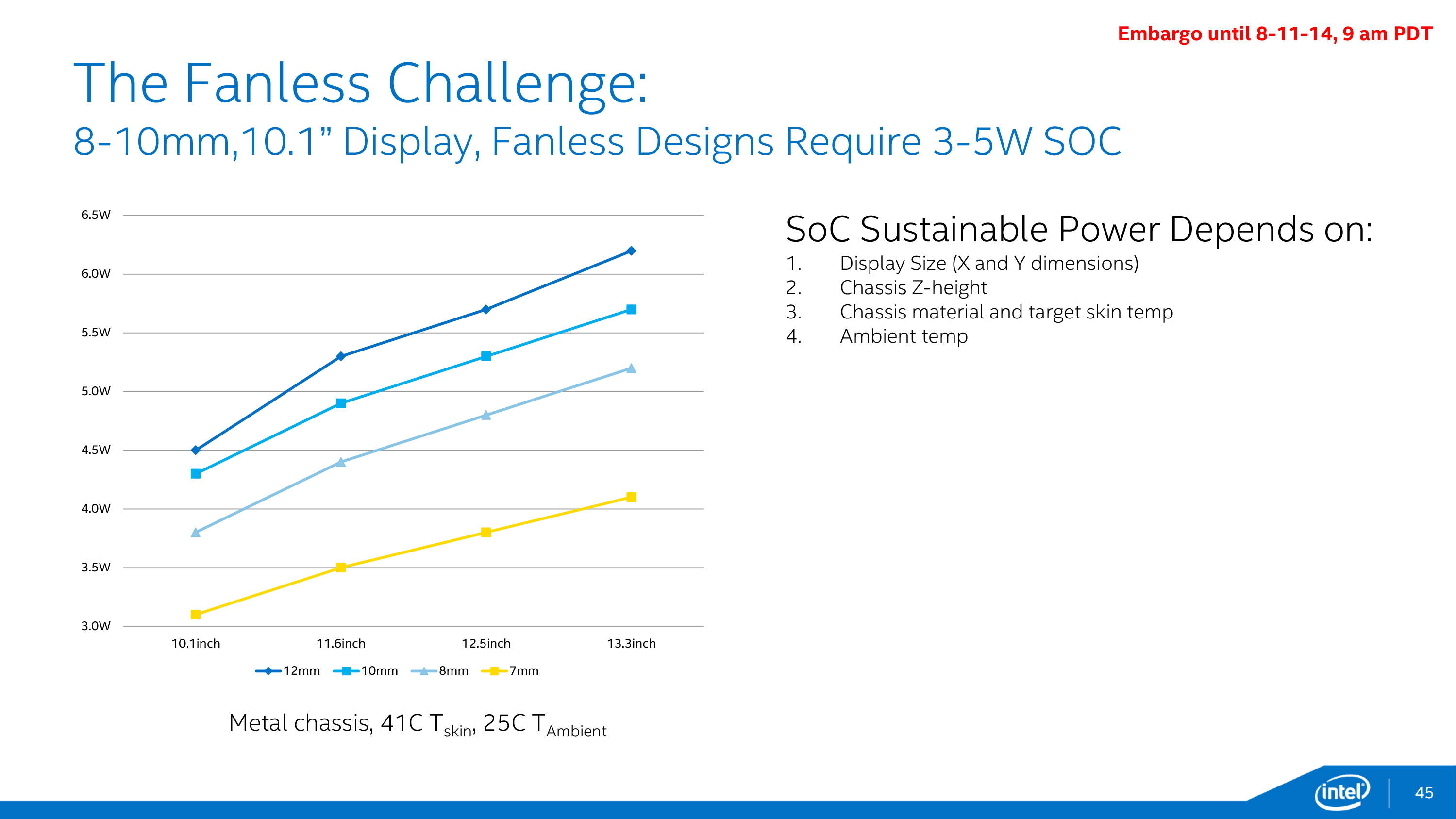
When it comes to building and configuring Core M, Intel likes to refer to their efforts as the “Fanless Challenge,” reflecting the fact that their biggest goal with Core M is to comfortably get the processor in to 10” tablets under 10mm in thickness that are passively cooled. A big part of getting into such a device is meeting the heat dissipation limitations of the form factor – a 10” tablet under 10mm would require a sub-5W SoC – which is where a lot of Intel’s engineering efforts have gone. Broadwell’s performance optimizations, the GPU optimizations, GPU duty cycling, and the 14nm process all contribute to getting a Core CPU’s power consumption down to that level.
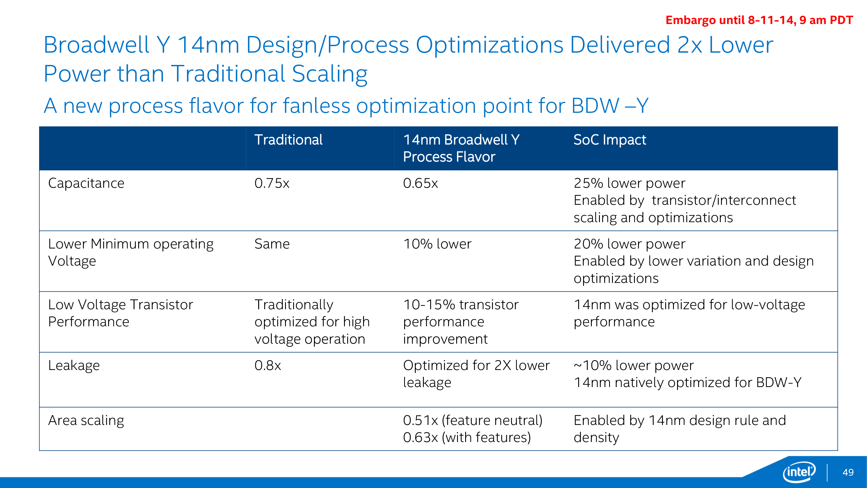
But even that’s still not enough, and for Core M Intel went so far as to give Broadwell-Y its own die and design a low-power optimized version of their 14nm process just for it. This variant is designed to further reduce power consumption by optimizing the resulting transistors for lower power, lower voltage, lower clockspeed operation. By doing this Intel was able to further reduce power consumption in all of the major areas over what would be a traditional 14nm Intel process.
In the resulting 14nm Broadwell-Y process, voltage, capacitance, and leakage were all improved over the traditional 14nm process. Capacitance was reduced by 15%, minimum operating voltages by 10%, and leakage was improved to the point that it reduced SoC power consumption by 10%. The combination of all of these factors serves to significantly lower power consumption over what Intel’s traditional 14nm process would provide.
Working in concert with Broadwell-Y’s 14nm process, Intel has made a number of other changes to further reduce power consumption. Some of these are reflected in Broadwell’s overall design and others are unique to Broadwell-Y, such as using a lower TjMax for Broadwell-Y. By reducing the maximum operating temperature of the chip Intel has been able to realize further power savings by further reducing voltage and decreasing the maximum amount of temperature-dependent leakage the SoC will experience.
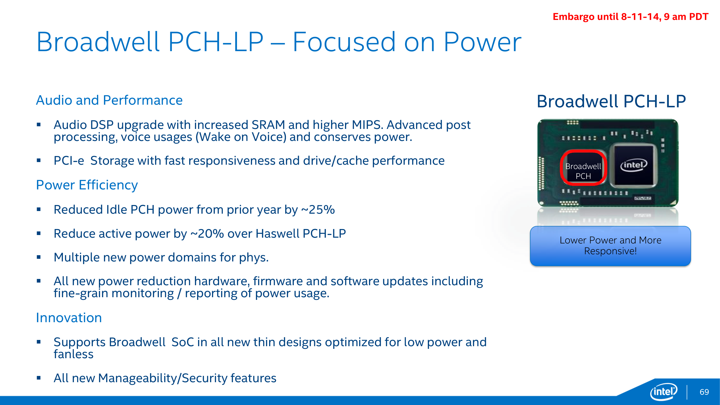
Meanwhile Broadwell-Y’s partner in crime, the on-package PCH, has received its own optimizations to reduce power consumption on the SoC’s total power consumption. The PCH itself is not much of a power hog in the first place – it’s still made on Intel’s 32nm process for this and cost reasons – but with such a strong focus on power consumption every watt ends up counting. As a result the Broadwell PCH-LP has seen optimizations that cut its idle power consumption by 25% and its active power consumption by 20%. Further improvements to the PCH’s monitoring hardware also mean it’s more responsive and can be controlled to a finer degree than the Haswell PCH-LP, and Intel has upgraded to a faster audio DSP to improve performance and reduce power consumption there as well.
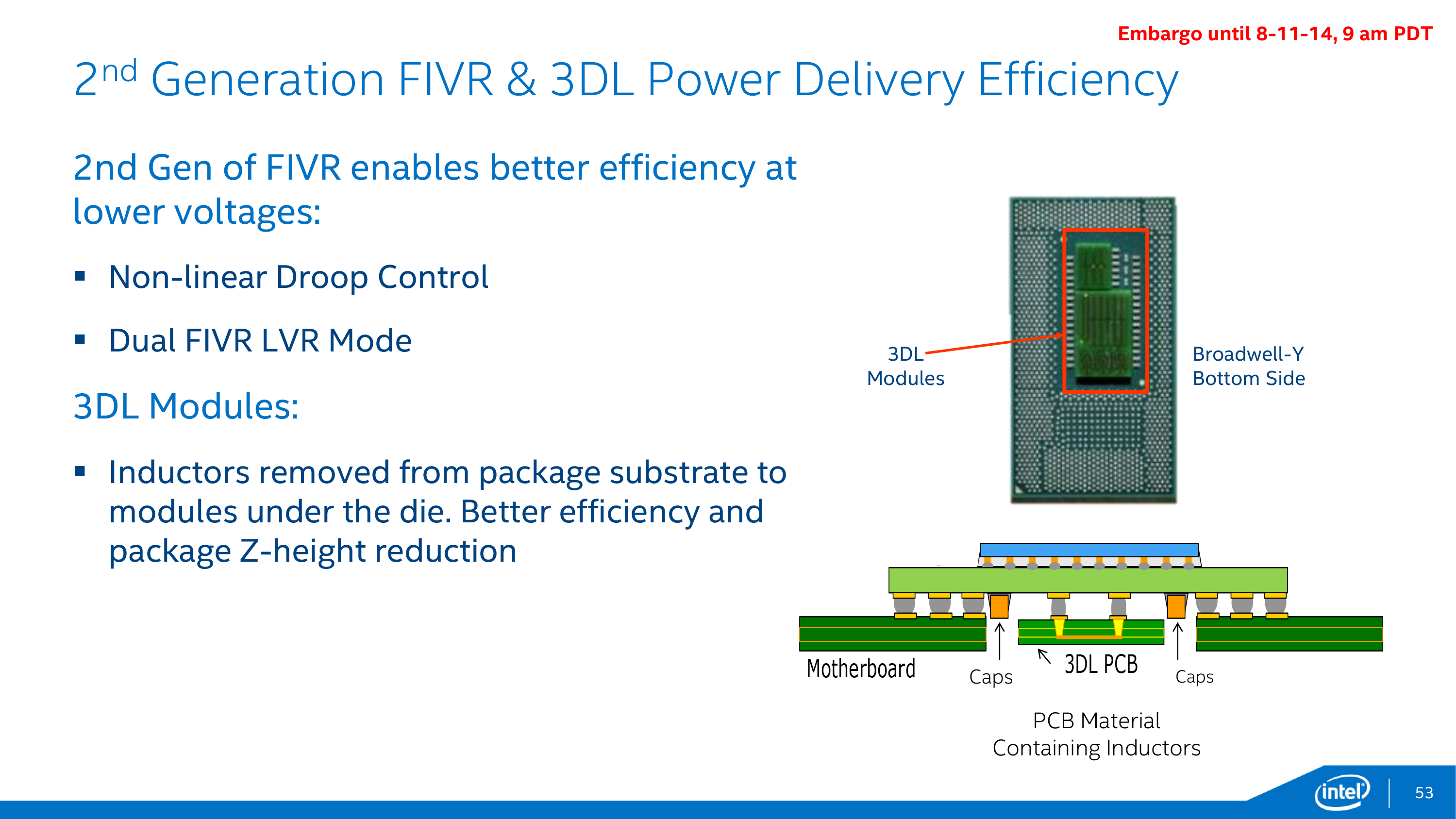
Feeding all of that silicon in turn is Intel’s second generation Fully Integrated Voltage Regulator (FIVR), which further builds off of Intel’s other optimizations. The 2nd gen FIVR has been tuned for Broadwell-Y’s lower voltages, making the FIVR itself more efficient when delivering power at those voltages. To accomplish this Intel has implemented non-linear vDroop control, which is designed to better control the voltage when workload changes would cause voltage overshoots that waste power. And when even the 2nd gen FIVR isn’t efficient enough, this latest FIVR offers a second mode (LVR Mode) for low voltage/workload situations where the FIVR can be partially bypassed to reduce the FIVR’s power consumption.
Interestingly Broadwell-Y also sees the voltage regulation inductors redesigned and relocated in both the name of power efficiency and space efficiency. We’ll get to the case of space efficiency in a moment, but for power efficiency the new 3D inductors (3DLs) have been placed on the underside of the package, allowing the use of more efficient inductors that waste less power.
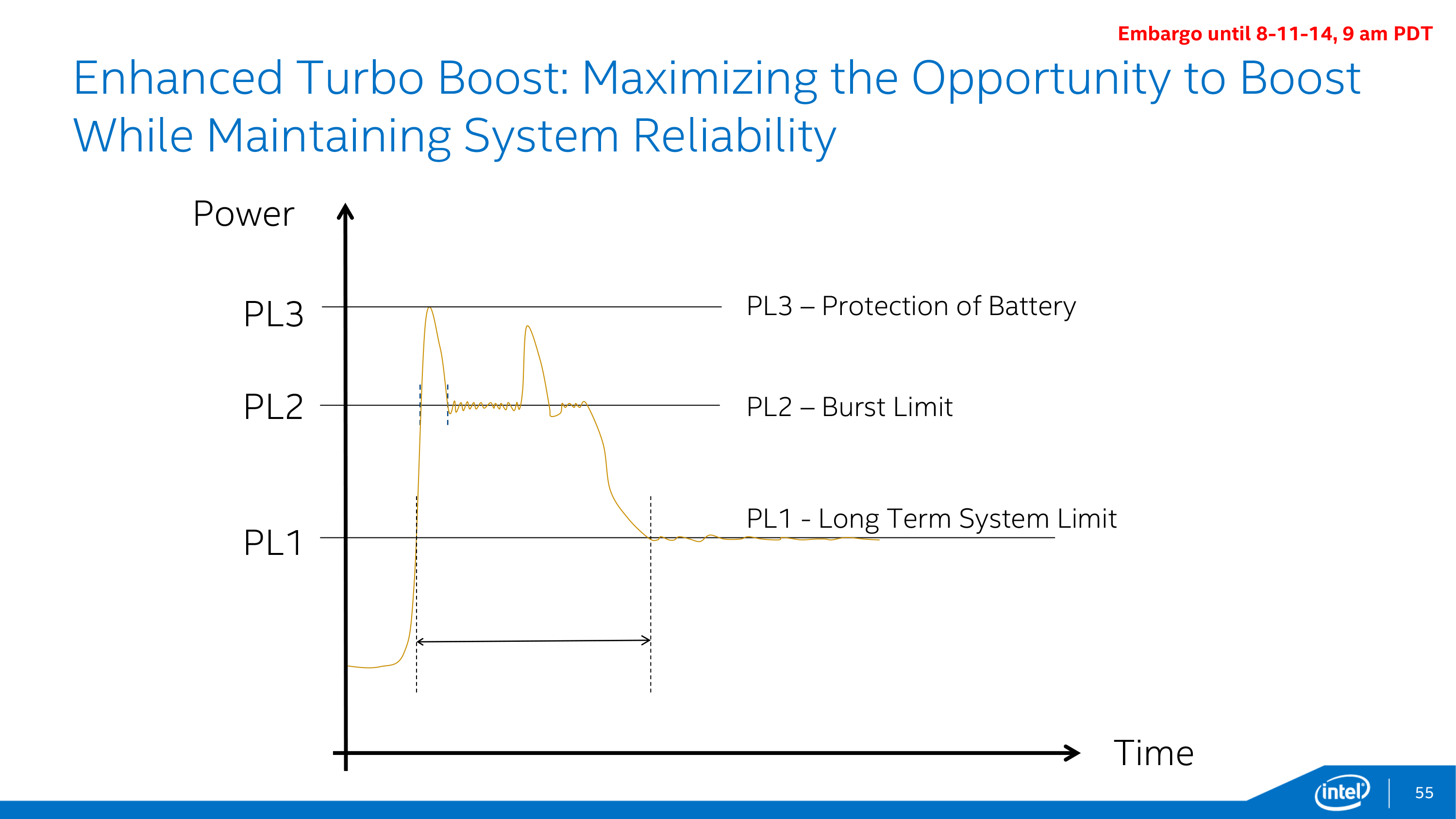
This brings us to the final element of Intel’s power optimization efforts, which involve further adjustments to turbo boost as part of Intel’s “hurry up and go to sleep” motto. New for Broadwell-Y is a 3rd power state, PL3, which allows for even greater turbo boosting, but for only a very limited period of time – on the order of milliseconds. PL3 represents the maximum amount of power the device battery can deliver, and while it’s okay to reach this value sparingly, PL3 is a fast drain that is very hard on the battery. The existence of PL3 in this case is as much for battery protection as it is for performance; it allows devices to tap into PL3 power levels on occasion, all the while allowing PL2 (the regular burst limit) to be defined at a safer value below the battery’s limit. Put another way, by knowing PL3 devices know how to stay farther away from it, which in the long run is what’s best for battery reliability.


158 Comments
View All Comments
crispbp04 - Monday, August 11, 2014 - link
Intel has something impressive in the works with Broadwell (at least on paper). I can't wait to get a Broadwell based Surface Pro. Assuming that Microsoft improves an already impressive hardware design from the sp3, the Broadwell iteration will likely be my next computer purchase.frostyfiredude - Monday, August 11, 2014 - link
I have a feeling SP4 will be fundamentally the same design as SP3 save for minor tweaks and improvements. SP3 was clearly designed for a processor with the kind of power profile Broadwell is set to deliver rather than the current Haswell profile. It will be interesting to see which set of SKUs Microsoft will put in the SP4, Core M or Broadwell ULT. Core M has a number of obvious benefits for power and area efficiency, but will it be powerful enough for their market with some features reduced from Haswell and Boradwell ULT.MonkeyPaw - Monday, August 11, 2014 - link
Pure speculation, but I think Intel might already be giving MS premium bins of Haswell for SP3, because SP3 is the only device to date to actually show off the ability to run premium Intel CPUs in a tablet format. Sure, MBA looks great, but SP3 took it to the next level.That said, I doubt that MS will use Core M in SP4, for the same reason we don't have Haswell-Y in SP3 (at least at the high end). It will probably be a step back in processing power to use one.
frostyfiredude - Tuesday, August 12, 2014 - link
Do we know what wattage the Broadwell ULT and Core M chips will be targeting? 15W TDP is clearly too high for the SP3 to handle so moving all SP4 chips to 11.5W like the current Haswell Y looks quite plausible at the moment, it just seems to be a matter of which version of Broadwell will have the 11.5W TDP.Samus - Wednesday, August 13, 2014 - link
15W is only a problem in SP3 to people who use it like a high performance computer (24x7 full load applications) but for general purpose use it barely warms up. We have people running Lightroom 8 hours a day on these things and like the Surface 2's (which I still have) they never got "hot" or "loud".That said, someone in the office infected their SP3 with some malware a few weeks ago (they literally owned the tablet not even 24 hours) and when they handed it to me, it was VERY hot with the fans whirling. Some 800kb task was using 100% of their CPU doing who knows what...at first I thought it was Cryptolocker but it turned out to be retrying a network connection. This was an i5 model, however, and it didn't seem to be throttling. The i3 will presumable run cooler, even at the same TDP.
What people need to keep in mind is these are mobile devices.
IntelUser2000 - Wednesday, August 13, 2014 - link
Broadwell ULT: 15WCore M(previously Broadwell-Y): 4.5W
vlad0 - Friday, August 15, 2014 - link
Isn't the core i3 version of the sp3 based on a Y series chip ?bebimbap - Monday, August 11, 2014 - link
agreed, Broadwell, and skylake will be vast improvements to PCs in general. Intel's Broadwell-Y announcement is all about "small, cool, efficient" while the recent FX-9590 seems more about "big, hot, gluttony" similar to the David vs Goliath story, the interesting part was the small one besting the big one. Ironically Intel is the bigger company. Hopefully AMD's new A1100 pans out as I don't want another Comcast, Microsoft, De Beers or Luxottica.wurizen - Monday, August 11, 2014 - link
well, if amd was as agressive as intel in shrinking dies or whathaveyou, then an AMD FX chip will probably be toe-to-toe to an intel i7-4930k or whatever the 6-core enthusiast intel chip is labeled. and not even die shrinks, but, also aggressive in producing a $500 cpu. imagine that. and you'd probably see an a10-7850k performance in a laptop by now. but, AMD seems content is sitting back and letting the other company do all the work, creating a path. as long as AMD doesn't completely die out, it's fine. we just need an alternative and AMD is the only one. so, go AMD. don't worry about broadwell. build it and we will come. be a niche. convert future x99 users to a future AMD product. and start from there.StevoLincolnite - Monday, August 11, 2014 - link
Except AMD can't be aggressive at shrinking dies.For one, die-shrinks costs money... For fab contracts, man-hours, research and possibly buying technology from other companies such as IBM.
AMD can't aggressively shrink dies anyway, they are at the mercy of fabrication companies like TSMC and Global Foundries, so what they can produce is limited to what they provide.
Intel has always been ahead of the industry in fabrication, the only way AMD can beat Intel is through something ground breaking (Like moving away from silicon?) or if Intel drops the ball, like they did with Netburst.
Or, AMD buys a fab company who is far ahead of Intel, which simply isn't going to happen.
Otherwise they can only compete on price and using an older more mature fabrication process allows them to do just that as the chips are much cheaper to produce, they just need to provide "Good enough" performance to mostly stay relevant, which the FX doesn't really do.