Testing Samsung 850 Pro Endurance & Measuring V-NAND Die Size
by Kristian Vättö on July 7, 2014 1:20 PM ESTV-NAND Die Size: Bigger Than What We Initially Thought
In our 850 Pro review, I did some calculations to estimate the die size of the second generation V-NAND based on the first generation V-NAND. As some of our clever readers pointed out, the die size does not scale perfectly with the die capacity because the peripheral circuitry cannot be scaled as aggressively as the capacity can be. As a result, my initial estimation ended up being way too small because I did not take the scaling of the peripheral circuitry into account.
Unfortunately, Samsung would not disclose the die size during the Q&A at the SSD Global Summit so I had to seek for an alternative way to figure out the correct die size. In the showroom, Samsung had the second generation 32-layer V-NAND wafer, which actually gives us everything we need to calculate a fairly accurate estimation of the die size.
The picture on top shows what the wafer looks like. It does not look any different from the typical 2D NAND wafer, which should not be a surprise given that the change happened deep inside. And no, the V-NAND wafer is not thicker than any normal wafer (at least not by eye) because the V-NAND stack is still in the order of microns.
As for the die size, I calculated 44 dies in the vertical direction, which means that with a 300mm wafer the depth of a single die is approximately 6.8mm.
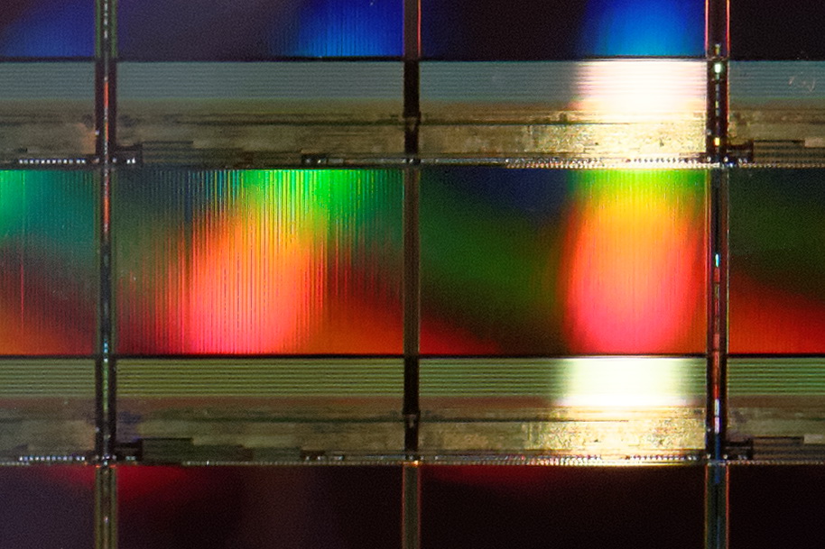
Courtesy of PC Perspective
To figure out the width of the die, you can either count the dies in the horizontal direction or go with the lazy route and just calculate the proportion of the depth and width. Allyn Malventano from PC Perspective was able to grab this awesome photo of the die itself, so I used the ruler tool in Photoshop to measure the size of the die along both X and Y axes and it appears that the width of the die is about 2.05 times its depth (note that it is a two-plane design). In other words, the die size is around 6.8mm x 14.0mm, which works out to be 95.4mm2.
| NAND Die Comparison | ||||
| Samsung 1st Gen V-NAND | Samsung 2nd Gen V-NAND | Micron 16nm NAND | Toshiba A19nm NAND | |
| Die Capacity | 128Gbit | 86Gbit | 128Gbit | 64Gbit |
| Die Size | 133mm2 | ~95.4mm2 | 173mm2 | 94mm2 |
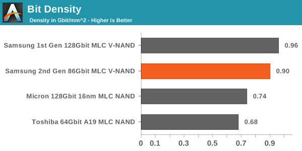
Here is an updated bit density graph. Even with the updated, larger die size, V-NAND is noticeably denser than 2D NAND, although the first generation appears to be more dense. I am guessing the smaller die size is better for yields (larger chips have higher probability of manufacturing errors), which makes the second generation more cost efficient despite the slightly lower density.


39 Comments
View All Comments
sonicmerlin - Friday, July 11, 2014 - link
But the cost per bit would be 16x less for Samsung as well, and they could sell at the same prices as they are now while raking in preposterous margins. There must be another reason they're not printing at at least the 2X node.pukemon1976 - Tuesday, July 15, 2014 - link
Thus the stagnation in innovation in a lot of industries. Smart phones are a great example of this. Look no further than Samsung and apple. Heck, Intel should throw AMD a bone or two so there isore competition in the x86 space.MrSpadge - Saturday, July 26, 2014 - link
The 40 nm process is very mature, but can't be used for anything power or performance critical anymore. Using these fabs for 3D NAND is making good use of them. I suppose they'll transition 3D NAND to smaller geometries once competitive pressure arises or once their 32 / 28 nm fabs are not completely utilized by other chips any more.jordanl17 - Thursday, August 28, 2014 - link
I just put 16x of the 512gb Samsung EVO 850's in an Equallogic PS6000 SAN. Raid 6 w/ hot spare. pretty sick. I'm going to get some cold spares for when these babies start to fail. but I'm hoping they last a long time!mdw9604 - Saturday, October 17, 2015 - link
How did that turn out?mrigi - Friday, September 19, 2014 - link
The worst scenario is not random write across the drive and not 100GiB per day but writing zillion times a day to a single sector like Chrome browser does with it's cache/history/bookmarks. That's the real world scenario. That is what kills drives regardless their firmwares that are cool on a paper only.Have you tested that? Is this what "write amplification" test does?
frostdude2025 - Sunday, November 9, 2014 - link
what do the two situations of writing 20 gb or 100 gb at 1.5 or 3.0 write amp even look like, always wondered thisIAEInferno - Sunday, September 18, 2016 - link
Hi I'm confused, it says that the limit is 150TB write limitation or 10 years warranty for the Samsung 850 Pro, how many years exactly does the 850 pro SSD at 512gb would last me if I'm just gaming while I store my movies, music, pictures, multiplayer games and etc. on a separate HDD while I just put my OS, some games and programs in the SSD?chrcoluk - Saturday, August 14, 2021 - link
Bait and switch again?Reviewer sample 1% for every 60 cycles.
My 850 pro 63 cycles and 98%. Which seems to be 30 cycles per 1% same as their MLC 2D drives lol.
With that said the drive is a few years old now, has been used in a ps4 pro which constantly records footage, and 2-3 years in my main PC. So to be at 98% of rated cycles is very nice for that length of time. Although its about 80% of the way to rated TB of warranty which was set very low by samsung.