Samsung SSD 850 Pro (128GB, 256GB & 1TB) Review: Enter the 3D Era
by Kristian Vättö on July 1, 2014 10:00 AM EST3D NAND: How It Works
To understand how 3D NAND helps to keep Moore's Law in action, we first need to go in-depth with the structure. Before we begin, there are a couple of disclaimers I want to get out. First of all, every manufacturer has a different 3D NAND structure, so to avoid information overflow and confusion, I will only talk about Samsung's structure for now. When other manufacturers are ready with their 3D NAND products, I will provide a similar analysis of their structure. Secondly, there is not much detailed information about Samsung's 3D NAND, or V-NAND as they call it, so I am mostly basing my analysis on The Memory Guy's blog post (also known as Jim Handy, a respected semiconductor analyst).

What you are seeing above is a 5-layer 3D NAND string based on Samsung's TCAT (Terabit Cell Array Transistor) structure. It consists of a total of ten cells and similar to 2D NAND each cell is capable of holding one, two or three bits of data depending on whether the NAND is SLC, MLC or TLC. Samsung's current (i.e. second) generation V-NAND has 32 layers, meaning that it is simply a taller tower but to keep the graph easily readable I decreased the number of layers to five.
There is one fundamental difference between Samsung's V-NAND. With 2D NAND, the charge was stored in a conductive floating gate but as you can see in the graph above, there is not one in Samsung's V-NAND. Instead Samsung uses a design called Charge Trap Flash (CTF), which means that the charge is stored in an insulator, which is silicon nitride in this case.
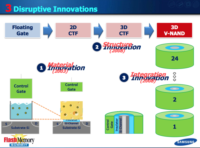
Some of you might remember this rather hilarious slide we used in our V-NAND announcement article and I now have an explanation as to why Samsung used cheese in in (yes, it indeed is cheese). A traditional floating gate works pretty much like a bucket of water. As long as there is not a hole in the bucket, the water stays there without an issue. However, if you get even a tiny hole in the bucket, all the water will sooner than later escape through that hole. It is the same with a floating gate because if there is a hole in the insulating material around it (Inter Poly Dielectric and tunnel oxide), all the electrons in the floating gate will escape through that as the floating gate is conductive and the electrons can move freely. As I mentioned on the previous page, this is exactly what happens when NAND is cycled and wears out because the stress caused by the programming operation causes the insulators to lose their insulating characteristics.
With Charge Trap Flash that does not happen because the electrons reside in an insulator. Samsung compared the bucket of water idea to cheese, meaning that if there is a hole the cheese will not just pour out from it like water would.
As a result, Charge Trap Flash increases endurance as it is not as vulnerable to wear out. I am also told that CTF does not require as high programming voltages as floating gates do (up to 20V), which reduces the stess on the insulators. I wonder if this is simply because the insulators do not have to be that thick anymore (a miminum of 7nm for tunnel oxide and 12nm for ONO) because the charge trap is not as dependent on the surrounding insulators as floating gate is. The reason why such a high voltage is needed for 2D NAND programming is the thickness of the tunnel oxide because otherwise the electrons cannot tunnel through (remember, the electrons are shot through an insulator). On the other hand, the tunnel oxide cannot be made any thinner than 7nm or otherwise data retention takes a massive hit (NAND is really an engineers dream, isn't it? Touch one thing and you break another).
Another interesting tidbit regarding Samsung’s V-NAND is the usage of a high-K dielectrics. IMFT did a similar switch when they moved to 20nm node but all the other manufacturers, as far as I know, have stayed with an inter poly dielectric (IPD) design. I went into detail about high-K dielectrics in our Crucial MX100 review but I will provide a quick summary here. Basically, a high-K dielectric is a material with a high dielectric constant, which is quite surprisingly known as K. The benefit of a high-K dielectric over a normal dielectric (like oxide-nitride-oxide i.e. ONO in NAND) is that it provides a higher capacitance between the word and bitlines. Similar to 2D NAND, the capacitance between the control gate and the floating gate, or charge trap in the case of V-NAND, is still the key factor for operation. The usage of high-K dielectrics gives Samsung a bit more headroom in terms of vertical scaling as layers can be stacked closer to each other and it also improves endurance as high-K dielectrics have less leakage compared to normal dielectrics.
Otherwise the basics of V-NAND are very similar to 2D NAND. To program a cell, the bitline is grounded (i.e. held at 0V) while a high voltage is placed on the wordline. That makes the electrons that are floating in the bitline to tunnel through the silicon dioxide to the charge trap a.k.a. silicon nitride.

I made a very simple graph of V-NAND programming, which should help you to understand the process. The elements are the same as in the tower graph with the difference that it is just one layer and I cut the tower in half to fit it on the page. The purple balls are electrons.
Reading from V-NAND works exactly the same as with 2D NAND. The wordline of the cell-to-be-read is held at 0V while different voltages are applied on the bitline. Once the correct voltage is found, the cell will conduct and the sense amp will read the data depending on what the voltage was (the voltage determines the voltage state, i.e. what the value is).


160 Comments
View All Comments
beginner99 - Tuesday, July 1, 2014 - link
Sounds great until you see the price. Even for an enthusiast a crucial MX100 is probably the more reasonable choice. It's half the price...juhatus - Tuesday, July 1, 2014 - link
Yeah, the most important factor of a SATA SSD is the price, not how it will saturate the 550Mb limit in a scenario that will never happen for most consumers. Now even a mention on the first page, eh? Please put a little pressure for the manufacturers to move on to M.2 and NVME.**In the Midnight hour, She cried more, more, more!!**
boogerlad - Tuesday, July 1, 2014 - link
Are you guys going to review the SM1715? Really curious to see how it stacks up against the Intel, especially in client workloads.pesho00 - Tuesday, July 1, 2014 - link
I realy hoped to see 2,3,4 TB drives with this technology :(But we will weith ;)
Nice drive, not so nice price ;)
MrSpadge - Tuesday, July 1, 2014 - link
Not much point in offering them now if you consider the price of the 1 TB version.Samus - Tuesday, July 1, 2014 - link
Those Koreans...they're just killer engineers.trumanhw - Tuesday, July 1, 2014 - link
I don't get it. I get about 505 read and 495 write on Evo. This goes up by TEN percent in performance and then all but DOUBLES the price?I'm confident someone here has understanding of this I'm missing--please reply and just point me to the parts that change my view.
Thanks
hojnikb - Tuesday, July 1, 2014 - link
Your EVO has worse endurance, lower IOPS, lower consistency and most of all lower Write speeds (495MB/s write is due to trick called turbowrite).Sequential speeds are only a part of the story.
emn13 - Tuesday, July 1, 2014 - link
I always wonder who this kind of drive is supposed to be aimed at. Yes, it's fast; but the competition is fast enough that I really can't imagine anyone *noticing* the difference outside of artificial extremely heavy non-stop I/O. And I don't mean light-load non-stop, I mean I/O's maxed out non-stop so the drives can't take time to garbage collect.So... a power user is unlikely to notice much difference outside of short bursts of high-I/O apps, and as the rather heavy 2011 light load demonstrates, the drives are already maxing out there too. I just can't think of a real-world load where a human being would notice the performance difference and care about it; that would imply a performance difference of around a factor 2.
So we're left with a super fast drive (good for bragging rights, but what else?), but some apparently intentionally missing features like power-loss protection. Why would even a heavy user choose this over, say, samsungs own 840 EVO, or crucial's MX100/M500?
I just don't see the value here. To me this looks like microoptimization and losing sight of the bigger picture.
Price matters. Features matter. Performance - only until you're fast enough.
hojnikb - Tuesday, July 1, 2014 - link
Kinga agree with this. If you REALLY need every bit of performance, you won't be looking for SATA drives at all.This probobly has a nieche.
But mainstream drives are really fast enough these days for most people.