Samsung SSD 850 Pro (128GB, 256GB & 1TB) Review: Enter the 3D Era
by Kristian Vättö on July 1, 2014 10:00 AM ESTWhy We Need 3D NAND
For years, it has been known that traditional NAND (i.e. 2D NAND) is running on its last legs. Many analysts predicted that we would not see NAND scaling below 20nm because the reliability would simply be too low to make such a small lithography feasible. However, thanks to some clever engineering on both hardware and firmware sides NAND has scaled to 15nm without any significant issues but now the limit has been reached for real. To understand the limits of 2D NAND scaling, let's say hello to our old good friend Mr. N-channel MOSFET.

Unfortunately the diagram above is a bit too simplified to truly show what we need, so let's look at a real cross-section photo instead:
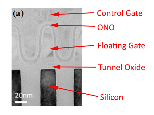
Let me walk you through the structure first. At the top is the control gate, which is a part of a structure known as a wordline. In a standard NAND design the control gate wraps around the floating gate and the two gates are separated by an insulating oxide-nitride-oxide layer (i.e. ONO), which is sometimes called Inter Poly Dielectric (IPD). Under the floating gate is the tunnel oxide, which is also an insulator, followed by the silicon substrate that acts as the bitline.
The reason why the control gate is wrapped around the floating gate is to maximize capacitance between the two. As you will soon learn, the capacitance between the gates is the key factor in NAND as it means that the control gate can control the floating gate.
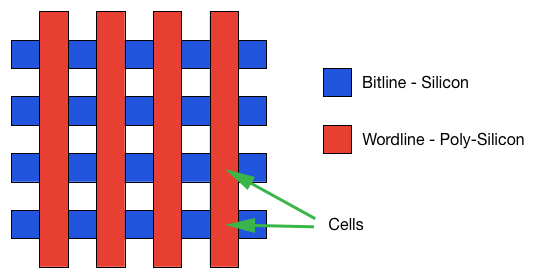
The purpose of bitlines and wordlines can be rather difficult to understand when looking at a cross-section, so here is what it all looks like from the top. Basically, bitlines and wordlines are just lines going in perpendicular directions and the floating gate and other materials reside between them.
When programming a cell, a high voltage of around 20V is applied to the wordline of that cell. Of course, the problem is that you cannot apply voltage to just one cell because the whole wordline will be activated so in order to select a specific cell, the bitline of that cell is held at 0V. At the same time, the neighbouring bitlines are charged to about 6V because this increases the capacitance between the bitline and floating gate, which is turn negates enough of the capacitance between the control and floating gate that the electrons cannot tunnel through the tunnel oxide. This is crucial because if all the bitlines were held at 0V, then all the cells along that wordline would be programmed with the same value.
To erase a cell, a reverse operation is performed by keeping the wordline at 0V while issuing a ~20V voltage on the bitline, which makes the electrons flow in the opposite direction (i.e. from the floating gate back to the bitline/silicon).
The way NAND is programmed and erased is also its Achilles' Heel. Because such high voltage is needed, the insulators around the floating gate (i.e. ONO and tunnel oxide) wear out as the NAND goes through program and erase cycles. The wear out causes the insulators to lose their insulating characters, meaning that electrons may now be able to escape the floating or get trapped in tunnel oxide during a program or erase. This causes a change in the voltage state of the cell.
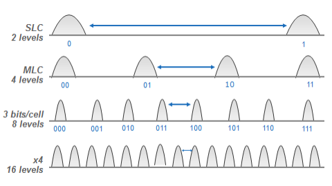
Remember, NAND uses the voltage states to define the bit value. If the charge in the floating gate is not what it is supposed to be, the cell may return an invalid value when read. With MLC and TLC this is even worse because the voltage states are much closer to each other, meaning that even minor changes in the voltage state may cause the voltage state to shift from its original position, which means the cell value will also change. Basically, MLC and TLC have less room for voltage state changes, which is why their endurance is lower because a cell that cannot hold its charge reliably is useless.
Now that we have covered the operation of NAND briefly, let's see what this has to do with scaling. Here is the same cross-section as above but with some dimensions attached.
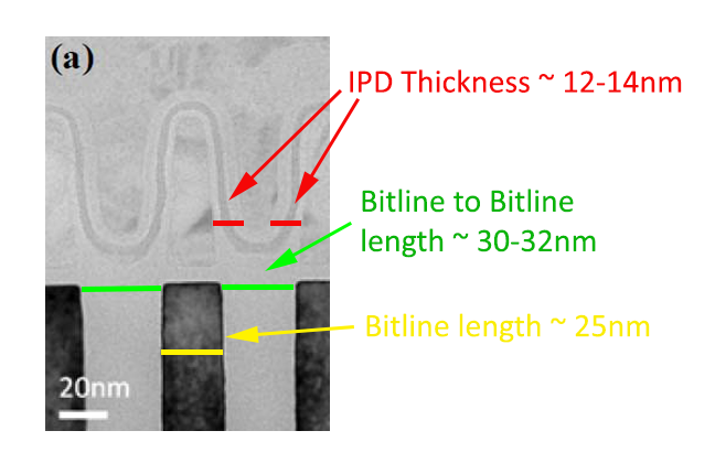
That is what a cross-section of a single cell looks like. When NAND is scaled, all these dimensions get smaller, which means that individual cells are smaller as well as the distance between each cell. The cross-section above is of IMFT's 25nm NAND (hence the bitline length of 25nm), so it is not exactly current generation but unfortunately I do not have any newer photos. There is no general rule to how much the dimensions shrink because 16nm simply means that one of the lengths is 16nm while others may not shrink that much.
The scaling introduces a variety of issues but I will start with the cell size. As the cell size is shrunk, the size of the floating gate is also shrunk, which means that the floating gate is able to hold less and less electrons every time the process node gets smaller. To put this into perspective, Toshiba's and SanDisk's 15nm NAND is stores less than 20 electrons per NAND cell. With TLC, that is less than three electrons per voltage state, so there is certainly not much headroom for escaped electrons. In other words, the cell becomes more vulnerable to the IPD and tunnel oxide wear out because even the loss of one electron can be vital to the voltage state.
The second issue is the proximity of the cells. The key factor in NAND is the capacitance between the control and floating gate but as the cells move closer to each other through scaling, the neighboring cells will also introduce capacitive coupling. In simpler terms, the neighboring cells will interfere more as the distance between the cells shrinks. The obstacle is that the interference varies depending on the charge of the neighbouring cell, so there is no easy way to exclude the intereference. This in turn makes programming harder and more time consuming because a higher voltage will be needed to achieve the sufficient capacitance between the control and floating gate to make the eletrons tunnel through the oxide.
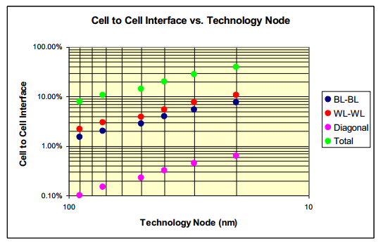
The graph above outlines historic rate of how cell to cell intereference increases through die shrinks. At 90nm, the interference was only around 8-9% but at 20nm it is a rather significant 40%. The interference means that 40% of the capacitive coupling comes from the other cells, making it very hard to control the gate you are trying to program or read. Fortunately as a result of some clever engineering (i.e. an airgap between the wordlines), the intererence is only about 25% at 25nm, which is much more managable than the 40% the historic rate would have given us.
The above can be fairly tough to digest, so let's do a simple analogy that everyone should be able to understand. Imagine that you have a bunch of speakers with each playing a different song. When these speakers are relatively large and far away from each other, it is easy to properly hear the song that the speaker closest to you is playing. Now, what happens if you bring the other speakers closer to the speaker you are listening? The other speakers will interfere and it becomes harder to tell your song apart from the others. If you turn down the volume or switch to smaller speakers with lower output volume, it becomes even harder to distinquish your song from the songs that the other songs that other speakers are playing. If you repeat this enough times, there will be a point when you are hearing your song as unclearly as the other songs.
The effect is essentially the same with NAND scaling. When the cells, or speakers in the analogy, move closer to each other, the amount of interference increases, making it harder to sense the cell or listen to the speaker. At the same time the size of the cell (or speakers) is shrunk, which further complicates the focus on one cell (or speaker).
That is NAND scaling and its issues in a nutshell. We have seen innovations such as airgaps between the wordlines to reduce cell-to-cell interference and a high K metal gate instead of a traditional ONO IPD to increase control gate to floating gate capacitance, but the limit has now been reached. However, like other semiconductors NAND must follow the Moore's Law in order to get more cost efficient. If you can no longer scale in the X and Y dimensions, what do you do? You hit the reset button and introduce the Z dimension.


160 Comments
View All Comments
GTVic - Tuesday, July 1, 2014 - link
Wondering if the 3D V-NAND has an effect on heat produced by each chip?Laststop311 - Wednesday, July 2, 2014 - link
If only this drive would of been a pci-e 3.0 x4 interface with nvme. We would of finally had a worthy upgrade. Yes it's performance is better than the 840 evo but you can get the 840 evo 1tb for 400 dollars even less if you catch it on sale. So you can get 2x 1tb 840 evo for almost the same price as 1 850 pro. If you compare an 840 evo with 25% OP to a regular 7% on the 850 the 840 evo looks just as good so 2x 825GB drives with 25% OP on each drive costs you 750-800 depending on the deal you get vs 700 for 1000GB. I would rather pay 800 for 1650GB than 700 for 1000GB with performance being nearly identical. I get an extra 650GB (which at 50 cents per GB is another 325 dollars worth of ssd) and tons of over provisioning to give the drive equal or better performance for only 100 dollars more (possibly less as the 840 evo has often sales)Sorry Samsung but 2x 1tb 840 evos with 25% provisioning gives me better or equal performance and a whole 650GB of extra storage for only 100 dollars more. At 50 cents per GB you get 325 dollars worth of more storage capacity for only 100 dollars more and thats with the 25% over provisioning which basically negates the performance increase of the new drives.
The only way samsung could of made this drive worth that money is if they had the drive on a pci-e 3.0 x4 interface with nvme instructions. I'm sure there will be tons of idiots who just buy it cause it's the latest drive. But if you use your brain you can see the 840 evo is still the best SATA drive when the cost/performance ratio is taken into account. 2x 1tb evo's in 25% OP mode gives you 1650GB and costs u 100 dollars extra or less and gives you the same performance or even better compared to 7% 850 pro 1000GB especially when raid 0 is taken into account. I'll take 1650GB over 1000GB if it's only 100 more and performance is equal or better easy choice.
Laststop311 - Wednesday, July 2, 2014 - link
Since samsung is stacking vertically now what they should of done is made a super huge 2tb drive to differentiate themselves from all these other drives. A 2tb drive for 1400 is a little more acceptable than 1tb for 700 simply because it's the only single drive with 2TB capacity.I can see great things happening with vertical stacked nand tho. When this process matures we should be seeing nand drives surpass spinning hard drives in capacity. When samsung has those 1tbit dies its planning for 2017 we should be able to have 8-12TB SSD's
althaz - Wednesday, July 2, 2014 - link
It's a new product and it's priced highly. Eager early adopters who want to move on to the latest and greatest will buy now, value-concious people will buy the 840s. Inventory of the 840s will get eaten up and the 850s will drop in price.This is what happens whenever any product is released, basically ever.
asmian - Wednesday, July 2, 2014 - link
Sorry, but neither this nor the EVO will get my money. Performance is all very well, even if only a tiny handful of users with extremely niche workloads will ever notice any difference, but all this extra reliability at a price premium means NOTHING without simple power loss protection. Restricting something so basic to "Enterprise" class products is the real gouging here by Samsung, not the price.If Crucial can provide that protection on the CHEAPEST drives in their class (M500/M550 and IIRC MX100 too) with performance that is not gimped as a balance, then there is no excuse for Samsung not to. This should be a no-compromise baseline for all SSDs going forward, and Anandtech should push hard for that - users should as well, by voting with their wallets and refusing to buy drives, however fast and powerful, that do not provide power loss protection as a basic feature.
bsd228 - Wednesday, July 2, 2014 - link
Though I agree it is a highly useful feature, it is far less significant to those of us using a good UPS. So I can't agree that it's a no compromise feature.romrunning - Wednesday, July 2, 2014 - link
What you aren't taking into account is the fact that the 850 Pro has MUCH higher endurance, and it's also more consistent. Those two items bring it more into the Intel DC 3500/3700 series type of class. It's not just a sheer performance comparison....and if you thing the 850 Pro is expensive, price out the larger Intel DC S3700 drives.
FunBunny2 - Wednesday, July 2, 2014 - link
"Real" Enterprise SSDs don't even have an MSRP. You negotiate with the vendor, and hope for the best. Now that Texas Memory is in IBM, and Fusion-io in SanDisk, with Violin likely to go somewhere. The conundrum is V.NAND's impact on flattening the curve between Enterprise and Commodity/Retail. At one time, a mainframe had bespoke 14" behemoth hard drive subsystems (in the case of IBM, run by the equivalent of a PDP-x). In due time, binned commodity 3.5" drives are now used.Samsung could well be the driving force to regularize solid state storage. The remaining issue is whether the file system hand waving will be dumped in favor of direct NVM persistence? Samsung, or whoever, likely couldn't care less.
romrunning - Wednesday, July 2, 2014 - link
It's been enjoyable to see a lot of "new" flash memory storage vendors pop-up. More competition is always good in that enterprise space.I've been looking forward to having more SSDs options available to servers at much better pricing. Solid storage advances have a trickle-down effect. If I can put an array of these Samsung 850 Pros into a server and achieve near "enterprise" performance, then that forces Dell/HP/etc. to drop their own SSD pricing.
watersb - Wednesday, July 2, 2014 - link
Fantastic detail of 3D NAND design and why it matters. Thanks very much!