Samsung SSD 850 Pro (128GB, 256GB & 1TB) Review: Enter the 3D Era
by Kristian Vättö on July 1, 2014 10:00 AM ESTPerformance vs. Transfer Size
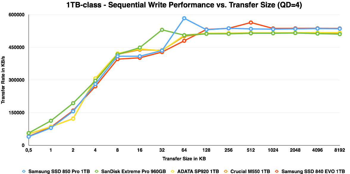
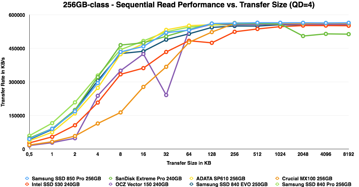
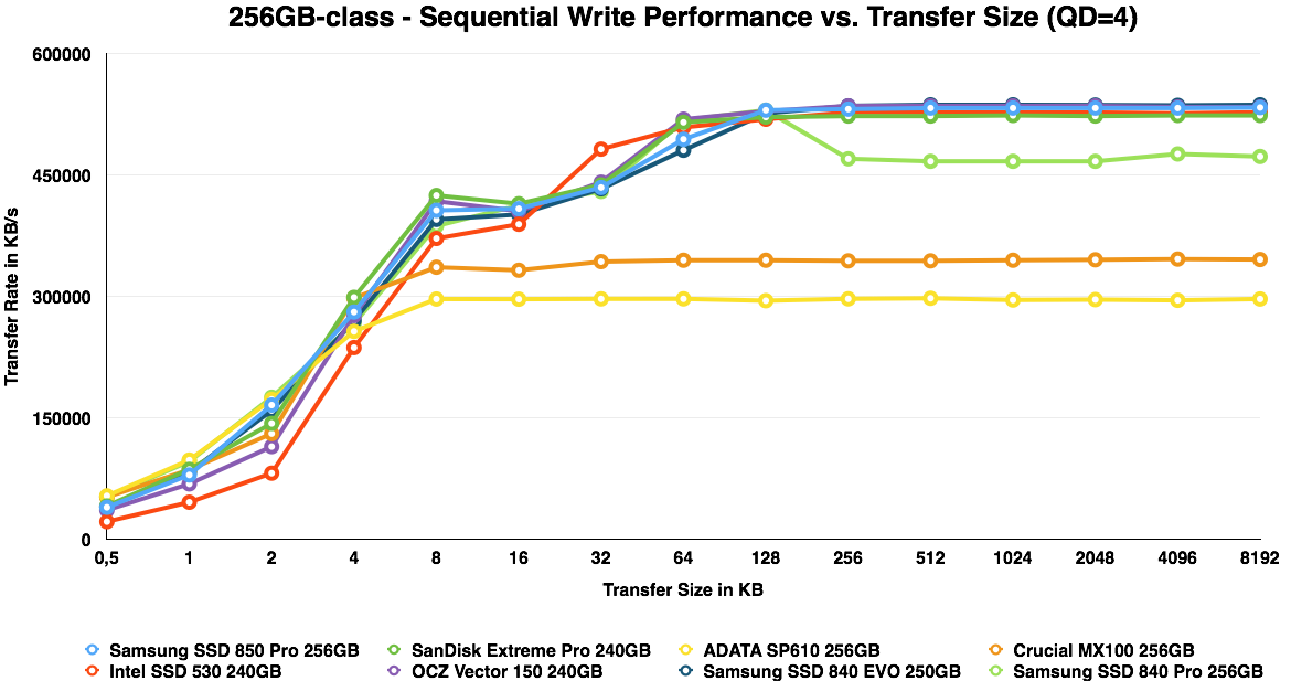
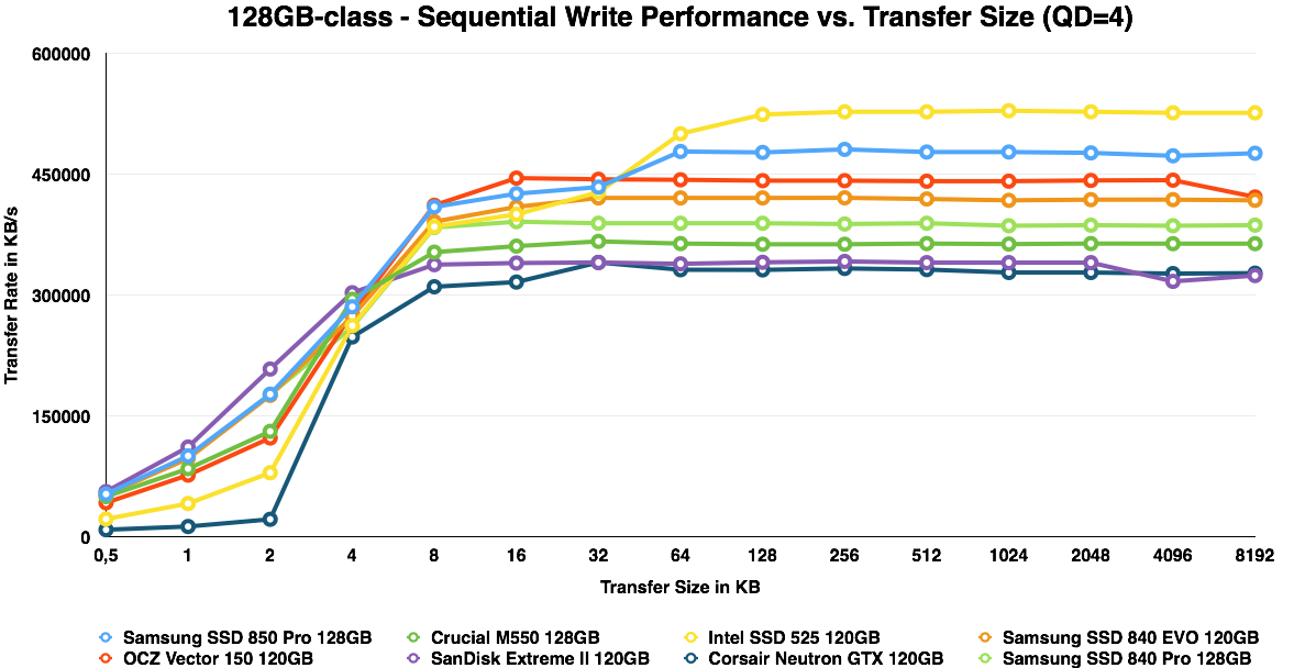
ATTO is a useful tool for quickly benchmarking performance across various transfer sizes. You can get the complete data set in Bench. To highlight the performance of each capacity, I decided to divide the ATTO graphs by each capacity, which should also make the graphs a bit more readable.

IO size scaling remain very similar to the 840 Pro and EVO. It is only at the 128GB capacity where the V-NAND provides a substantial advantage and the 850 Pro is almost as fast as the 120GB Intel SSD 525, which is a SandForce based drive, so its high performance is explained by ATTO's use of compressible data.


160 Comments
View All Comments
emvonline - Tuesday, July 1, 2014 - link
is the die size for the NAND chip 67mm^2? I assumed you measured it (pretty easy to do). I would think it would be much larger than thatGigaplex - Tuesday, July 1, 2014 - link
It's difficult to measure the die when multiple of them are on the same package.emvonline - Tuesday, July 1, 2014 - link
send me the package... I promise to have exact die size in a week ..... TEM cross sections in two weeks :-)Kristian Vättö - Tuesday, July 1, 2014 - link
Send me an email at kristian@anandtech.com and let's work this out :)extide - Tuesday, July 1, 2014 - link
Yes, 67mm^2, but remember that is 32 "deep"emvonline - Tuesday, July 1, 2014 - link
@extide: so you measured the die to be 67mm^2? how was this measured ? CSAM? XRAY? that seems odd to use such a small dies for SSD. and that would make it even smaller cell size than the one at ISSCC since it was 134 for a 128Gbit with 24 layers (periphery doesnt shrink as fast with lower density)Kristian Vättö - Tuesday, July 1, 2014 - link
No I didn't because I don't have the equipment to do that. The method I used to calculate the die size is explained on the fifth page of the review:http://www.anandtech.com/show/8216/samsung-ssd-850...
I'm not claiming that it is an accurate figure, hence the "~" sign in front of it. However, Samsung wouldn't disclose the die size when I asked them during the Q&A, so at this point I don't know for sure. However, I have a picture of the 32-layer wafer and once I get back home I'll do the math of the wafer to figure out the exact die size.
emvonline - Tuesday, July 1, 2014 - link
Got it thanks. I am mainly wondering about redundancy, extra blocks and ECC overhead.drwho9437 - Tuesday, July 1, 2014 - link
The micrograph you say is an "x-ray", is almost certainly a transmission electron microscopy image. Given the oxides are light it is a bright field image. It could technically be a SEM image but the resolution is a bit to high, so it most likely is a STEM image with a bright field detector.GTVic - Tuesday, July 1, 2014 - link
Perhaps time should be added as a cost efficiency factor. Presumably the die has to stay in the process much longer due to all the layers being added one at a time.