Samsung SSD 850 Pro (128GB, 256GB & 1TB) Review: Enter the 3D Era
by Kristian Vättö on July 1, 2014 10:00 AM ESTRandom Read/Write Speed
The four corners of SSD performance are as follows: random read, random write, sequential read and sequential write speed. Random accesses are generally small in size, while sequential accesses tend to be larger and thus we have the four Iometer tests we use in all of our reviews.
Our first test writes 4KB in a completely random pattern over an 8GB space of the drive to simulate the sort of random access that you'd see on an OS drive (even this is more stressful than a normal desktop user would see). We perform three concurrent IOs and run the test for 3 minutes. The results reported are in average MB/s over the entire time.
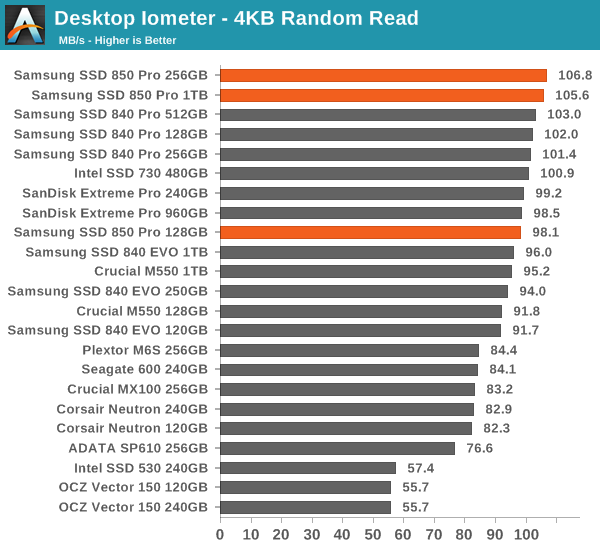
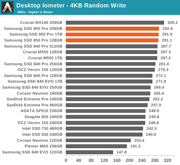
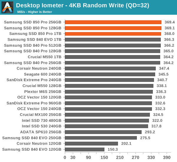
Random performance is also brilliant and the 850 Pro tops almost all of our benchmarks. It is no wonder why it is so fast in the Storage Benches.
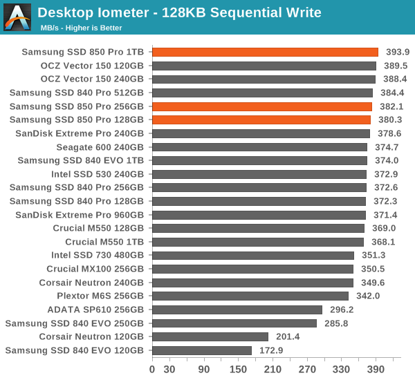
Sequential Read/Write Speed
To measure sequential performance we run a 1 minute long 128KB sequential test over the entire span of the drive at a queue depth of 1. The results reported are in average MB/s over the entire test length.
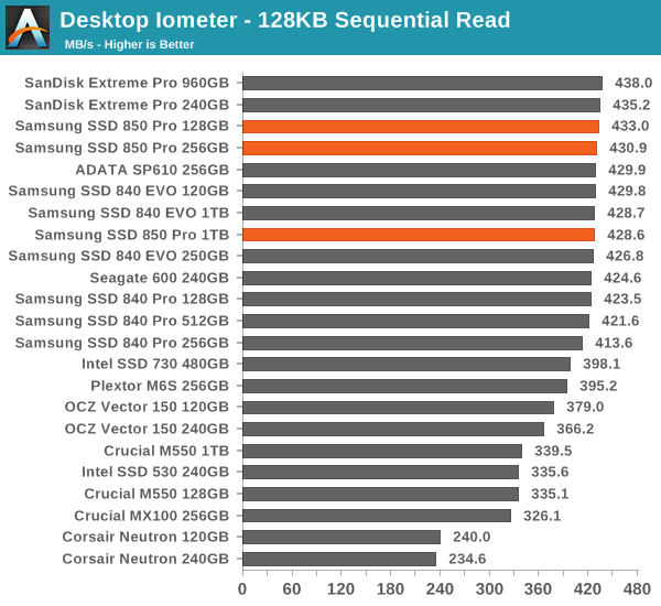
The same goes for sequential speeds. Of course, the differences are not substantial but nevertheless the 850 Pro is fast.
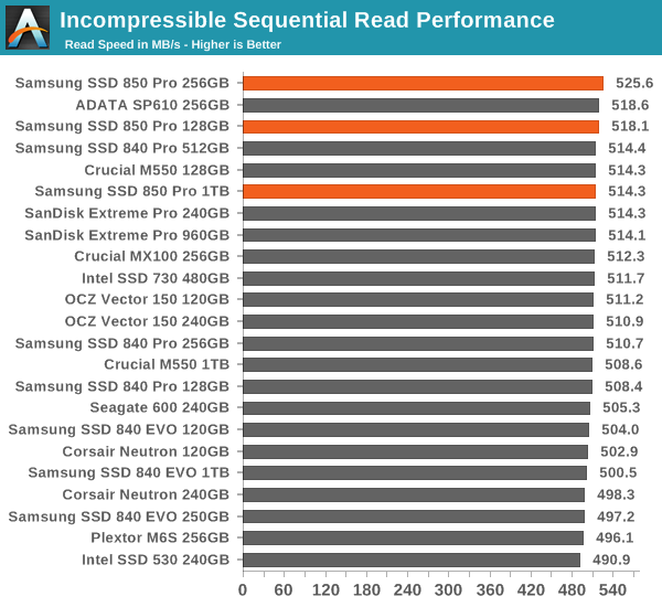
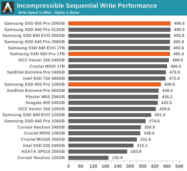
AS-SSD Incompressible Sequential Read/Write Performance
The AS-SSD sequential benchmark uses incompressible data for all of its transfers. The result is a pretty big reduction in sequential write speed on SandForce based controllers, but it doesn't impact most of the other controller much if at all.


160 Comments
View All Comments
emvonline - Tuesday, July 1, 2014 - link
is the die size for the NAND chip 67mm^2? I assumed you measured it (pretty easy to do). I would think it would be much larger than thatGigaplex - Tuesday, July 1, 2014 - link
It's difficult to measure the die when multiple of them are on the same package.emvonline - Tuesday, July 1, 2014 - link
send me the package... I promise to have exact die size in a week ..... TEM cross sections in two weeks :-)Kristian Vättö - Tuesday, July 1, 2014 - link
Send me an email at kristian@anandtech.com and let's work this out :)extide - Tuesday, July 1, 2014 - link
Yes, 67mm^2, but remember that is 32 "deep"emvonline - Tuesday, July 1, 2014 - link
@extide: so you measured the die to be 67mm^2? how was this measured ? CSAM? XRAY? that seems odd to use such a small dies for SSD. and that would make it even smaller cell size than the one at ISSCC since it was 134 for a 128Gbit with 24 layers (periphery doesnt shrink as fast with lower density)Kristian Vättö - Tuesday, July 1, 2014 - link
No I didn't because I don't have the equipment to do that. The method I used to calculate the die size is explained on the fifth page of the review:http://www.anandtech.com/show/8216/samsung-ssd-850...
I'm not claiming that it is an accurate figure, hence the "~" sign in front of it. However, Samsung wouldn't disclose the die size when I asked them during the Q&A, so at this point I don't know for sure. However, I have a picture of the 32-layer wafer and once I get back home I'll do the math of the wafer to figure out the exact die size.
emvonline - Tuesday, July 1, 2014 - link
Got it thanks. I am mainly wondering about redundancy, extra blocks and ECC overhead.drwho9437 - Tuesday, July 1, 2014 - link
The micrograph you say is an "x-ray", is almost certainly a transmission electron microscopy image. Given the oxides are light it is a bright field image. It could technically be a SEM image but the resolution is a bit to high, so it most likely is a STEM image with a bright field detector.GTVic - Tuesday, July 1, 2014 - link
Perhaps time should be added as a cost efficiency factor. Presumably the die has to stay in the process much longer due to all the layers being added one at a time.