AMD Kaveri Review: A8-7600 and A10-7850K Tested
by Ian Cutress & Rahul Garg on January 14, 2014 8:00 AM ESTLlano, Trinity and Kaveri Die: Compared
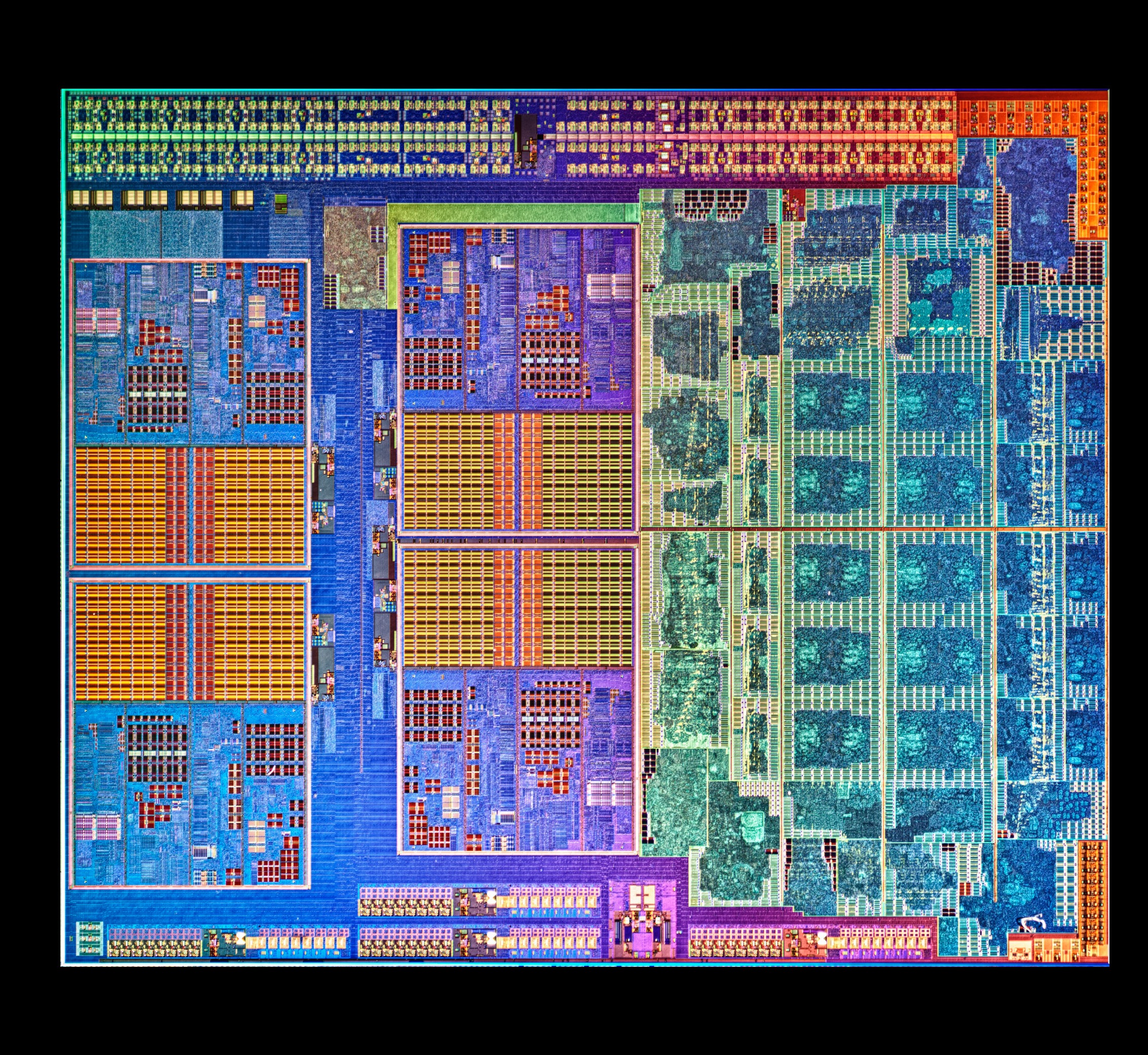
AMD sent along a high res shot of Kaveri's die. Armed with the same from the previous two generations, we can get a decent idea of the progression of AMD's APUs:
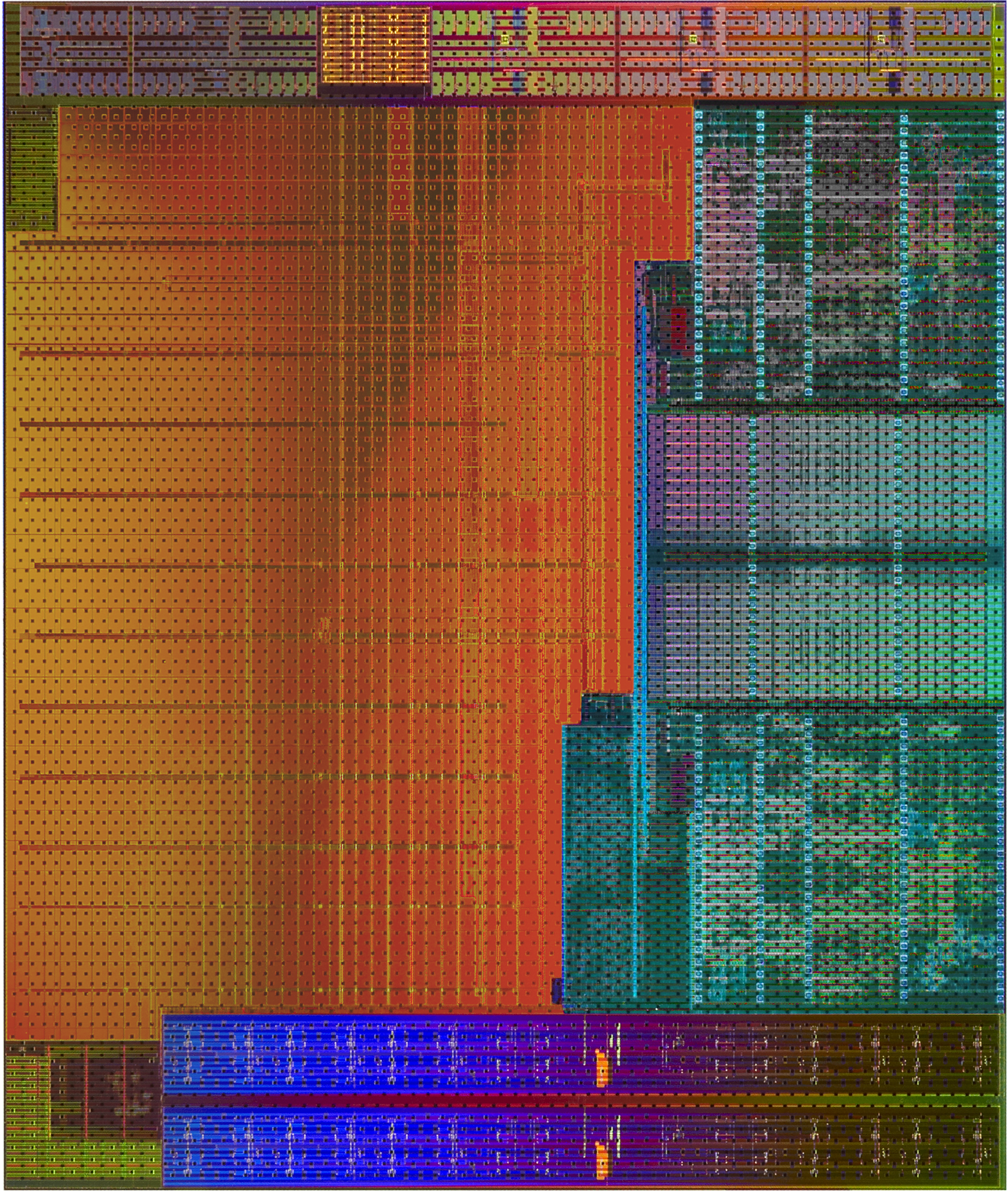
Llano, K10 Quad Core

Trinity and Richland Die, with two Piledriver modules and processor graphics
Kaveri, two modules and processor graphics
Moving from Llano to Trinity, we have the reduction from a fully-fledged quad core system to the dual module layout AMD is keeping with its APU range. Moving from Richland to Kaveri is actually a bigger step than one might imagine:
| AMD APU Details | ||||
| Core Name | Llano | Trinity | Richland | Kaveri |
| Microarch | K10 | Piledriver | Piledriver | Steamroller |
| CPU Example | A8-3850 | A10-5800K | A10-6800K | A10-7850K |
| Threads | 4 | 4 | 4 | 4 |
| Cores | 4 | 2 | 2 | 2 |
| GPU | HD 6550 | HD 7660D | HD 8670D | R7 |
| GPU Arch | VLIW5 | VLIW4 | VLIW4 | GCN 1.1 |
| GPU Cores | 400 | 384 | 384 | 512 |
| Die size / mm2 | 228 | 246 | 246 | 245 |
| Transistors | 1.178 B | 1.303 B | 1.303 B | 2.41 B |
| Power | 100W | 100W | 100W | 95W |
| CPU MHz | 2900 | 3800 | 4100 | 3700 |
| CPU Turbo | N/A | 4200 | 4400 | 4000 |
| L1 Cache |
256KB C$ 256KB D$ |
128KB C$ 64KB D$ |
128KB C$ 64KB D$ |
192KB C$ 64KB D$ |
| L2 Cache | 4 x 1MB | 2 x 2 MB | 2 x 2 MB | 2 x 2 MB |
| Node | 32nm SOI | 32nm SOI | 32nm SOI | 28nm SHP |
| Memory | DDR-1866 | DDR-1866 | DDR-2133 | DDR-2133 |
Looking back at Llano and Trinity/Richland, it's very clear that AMD's APUs on GF's 32nm SOI process had a real issue with transistor density. The table below attempts to put everything in perspective but keep in mind that, outside of Intel, no one does a good job of documenting how they are counting (estimating) transistors. My only hope is AMD's transistor counting methods are consistent across CPU and GPU, although that alone may be wishful thinking:
| Transistor Density Comparison | ||||||||
| Manufacturing Process | Transistor Count | Die Size | Transistors per mm2 | |||||
| AMD Kaveri | GF 28nm SHP | 2.41B | 245 mm2 | 9.837M | ||||
| AMD Richland | GF 32nm SOI | 1.30B | 246 mm2 | 5.285M | ||||
| AMD Llano | GF 32nm SOI | 1.178B | 228 mm2 | 5.166M | ||||
| AMD Bonaire (R7 260X) | TSMC 28nm | 2.08B | 160 mm2 | 13.000M | ||||
| AMD Pitcairn (R7 270/270X) | TSMC 28nm | 2.80B | 212 mm2 | 13.209M | ||||
| AMD Vishera (FX-8350) | GF 32nm SOI | 1.2B | 315 mm2 | 3.810M | ||||
| Intel Haswell 4C (GT2) | Intel 22nm | 1.40B | 177 mm2 | 7.910M | ||||
| NVIDIA GK106 (GTX 660) | TSMC 28nm | 2.54B | 214 mm2 | 11.869M | ||||
If AMD is indeed counting the same way across APUs/GPUs, the move to Kaveri doesn't look all that extreme but rather a good point in between previous APUs and other AMD GCN GPUs. Compared to standalone CPU architectures from AMD, it's clear that the APUs are far more dense thanks to big portions of their die being occupied by a GPU.


380 Comments
View All Comments
dbcoopernz - Tuesday, January 14, 2014 - link
I'd like an APU with enough GPU power to run all the high quality options in MadVR. Would make a very nice HTPC chip.thomascheng - Tuesday, January 14, 2014 - link
I think Mantle can make that happen, but will see how much support they get.MrSpadge - Tuesday, January 14, 2014 - link
Mantle has nothing to do with GP-GPU, that's not using DirectX anyway.JDG1980 - Tuesday, January 14, 2014 - link
My discrete 7750 couldn't handle Jinc scaling in MadVR (at least not without dropping frames on some 1080i test clips), so this is going to be another generation or two in the future.The PS4 APU could probably do it, if that was available in a generic PC form factor.
MrSpadge - Tuesday, January 14, 2014 - link
Add to that DDR4 and/or 4 memory channels, or at least a large on-package buffer like Crystal Well.yankeeDDL - Wednesday, January 15, 2014 - link
But the whole point of HSA is to get the GPU to do CPU work that it could do better (like FP).So you wouldn't need more CPU cores at all.
Look at it this way: AMD's CPU is less efficient than Intel's, while the GPU is more efficient.
Having a CPU-imbalanced APU, would put it in a tough(er) spot to compete against Intel. A GPU imbalanced, as Kaveri is, would improve the lead than it already has on the GPU side.
Now imagine that HSA kicks in, and the GPU lead translates directly in CPU lead ...
mikato - Wednesday, January 15, 2014 - link
This is true. I hope we see more articles as adoption of HSA starts to take hold.It is too bad they are far behind in CPU power, but AMD has the right strategy. Either way, some things are better done on the GPU. AMD just has more benefit than Intel to get things moving that way sooner with their GPU advantage and CPU disadvantage. Intel will have no choice but to follow that lead.
nissangtr786 - Tuesday, January 14, 2014 - link
http://www.extremetech.com/computing/174632-amd-ka...hsa does well on amd main thing they marketed in libreoffice.
Ryan Smith - Tuesday, January 14, 2014 - link
I'm normally not one to speak about other articles, but those are all OpenCL benchmarks. The OpenCL HSA driver won't be released for another quarter. And the HSA SDK is similarly far off.http://www.anandtech.com/show/7677/amd-kaveri-revi...
krumme - Tuesday, January 14, 2014 - link
What a bencmark of a review. I learned a lot. Great. Thanx.