NVIDIA Tegra K1 Preview & Architecture Analysis
by Brian Klug & Anand Lal Shimpi on January 6, 2014 6:31 AM ESTCPU Option 2: Dual-Core 64-bit NVIDIA Denver
Three years ago, also at CES, NVIDIA announced that it was working on its own custom ARM based microprocessor, codenamed Denver. Denver was teased back in 2011 as a solution for everything from PCs to servers, with no direct mention of going into phones or tablets. In the second half of 2014, NVIDIA expects to offer a second version of Tegra K1 based on two Denver cores instead of 4+1 ARM Cortex A15s. Details are light but here’s what I’m expecting/have been able to piece together.
Given the 28nm HPM process for Tegra K1, I’d expect that the Denver version is also a 28nm HPM design. NVIDIA claims the two SoCs are pin-compatible, which tells me that both feature the same 64-bit wide LPDDR3 memory interface.
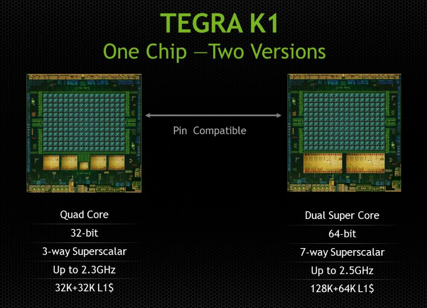
The companion core is gone in the Denver version of K1, as is the quad-core silliness. Instead you get two, presumably larger cores with much higher IPC; in other words, the right way to design a CPU for mobile. Ironically it’s NVIDIA, the company that drove the rest of the ARM market into the core race, that is the first (excluding Apple/Intel) to come to the realization that four cores may not be the best use of die area in pursuit of good performance per watt in a phone/tablet design.
It’s long been rumored that Denver was a reincarnation of NVIDIA’s original design for an x86 CPU. The rumor there being NVIDIA used binary translation to convert x86 assembly to some internal format (optimizing the assembly in the process for proper scheduling/dispatch/execution) before it hit the CPU core itself. The obvious change being instead of being x86 compatible, NVIDIA built something that was compatible with ARMv8.
I believe Denver still works the same way though. My guess is there’s some form of a software abstraction layer that intercepts ARMv8 machine code, translates and optimizes/morphs it into a friendlier format and then dispatches it to the underlying hardware. We’ve seen code morphing + binary translation done in the past, including famously in Transmeta’s offerings in the early 2000s, but it’s never been done all that well at the consumer client level.
Mobile SoC vendors are caught in a tough position. Each generation they are presented with opportunities to increase performance, however at some point you need to move to a larger out of order design in order to efficiently scale performance. Once you make that jump, there’s a corresponding increase in power consumption that you simply can’t get over. Furthermore, subsequent performance increases usually depend on leveraging more speculative execution, which also comes with substantial power costs.
ARM’s solution to this problem is to have your cake and eat it too. Ship a design with some big, speculative, out of order cores but also include some in-order cores when you don’t absolutely need the added performance. Include some logic to switch between the cores and you’re golden.
If Denver indeed follows this path of binary translation + code optimization/morphing, it offers another option for saving power while increasing performance in mobile. You can build a relatively wide machine (NVIDIA claims Denver is a 7-issue design, though it’s important to note that we’re talking about the CPU’s internal instruction format and it’s not clear what type of instructions can be co-issued) but move a lot of the scheduling/ILP complexities into software. With a good code morphing engine the CPU could regularly receive nice bundles of instructions that are already optimized for peak parallelism. Removing the scheduling/OoO complexities from the CPU could save power.
Granted all of this funky code translation and optimization is done in software, which ultimately has to run on the same underlying CPU hardware, so some power is expended doing that. The point being that if you do it efficiently, any power/time you spend here will still cost less than if you had built a conventional OoO machine.
I have to say that if this does end up being the case, I’ve got to give Charlie credit. He called it all back in late 2011, a few months after NVIDIA announced Denver.
NVIDIA announced that Denver would have a 128KB L1 instruction cache and a 64KB L1 data cache. It’s fairly unusual to see imbalanced L1 I/D caches like that in a client machine, which I can only assume has something to do with Denver’s more unique architecture. Curiously enough, Transmeta’s Efficeon processor (2nd generation code morphing CPU) had the exact same L1 cache sizes (it also worked on 8-wide VLIW instructions for what it’s worth). NVIDIA also gave us a clock target of 2.5GHz. For an insanely wide machine 2.5GHz sounds pretty high, especially if we’re talking about 28nm HPM, so I’m betting Charlie is right in that we need to put machine width in perspective.
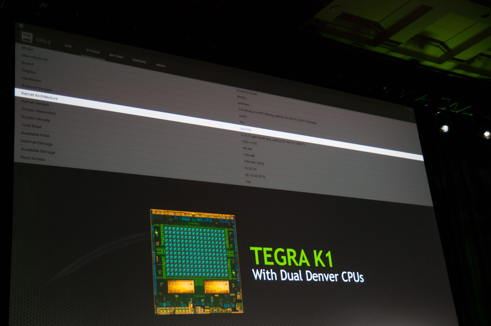
NVIDIA showed a Denver Tegra K1 running Android 4.4 at CES. The design came back from the fab sometime in the past couple of weeks and is already up and running Android. NVIDIA hopes to ship the Denver version of Tegra K1 in the second half of the year.
The Denver option is the more interesting of the two as it not only gives us another (very unique) solution to the power problem in mobile, but it also embraces a much more sane idea of the right balance of core size vs. core count in mobile.


88 Comments
View All Comments
jerrylzy - Tuesday, January 7, 2014 - link
Exactly. I don't see Loki726's point of gamers paying extra $ for Double Precision. AMD Cards are generally much cheaper at the same performance level, though at the cost of power consumption.Loki726 - Tuesday, January 7, 2014 - link
I mean compared to a world where AMD decided to rip out the double precision units. There are obviously many (thousands) other factors that do into the efficiency of a GPU.jerrylzy - Tuesday, January 7, 2014 - link
Unfortunately, instead of using VLIW 5, Qualcomm implemented new scalar architecture way back in adreno 320.Loki726 - Tuesday, January 7, 2014 - link
Yep, the have improved on it, but they started with the AMD design. My point was that the Qualcomm GPU is a better comparison point to a Tegra SoC than an AMD desktop part.ddriver - Wednesday, January 8, 2014 - link
The decision to chose Qualcomm in favor of Tegra would be based entirely on the absence of OpenCL support in Tegra. Exclusive cuda? Come on, who would want to invest into writing a parallel accelerated high performance routine that only works on like no more than 5% of the hardware-capable to run it devices? Not me anyway.The mention of the radeon was regarding a completely different point - that nvidia sacks DP performance even where it makes no sense to, and is IMO criminal to do so - the "gain" of such a terrible DP implementation is completely diminished by the loss of potential performance and possibility of accelerating a lot of professional workstation software. And for what, so the only spared parts - the "professional" products can have their ridiculous prices better "justified"? Because it is such a sweet deal to make a product 10% more expensive to make and ask 5000% more money for it.
Which is the reason AMD offers so much more value, while limp and non-competitive in the CPU performance, the place where computation is really needed - professional workstation software can greatly benefit from parallelization, and the much cheaper desktop enthusiast product actually delivers more raw computational power than the identical, but more conservatively clocked fireGL analog. Surely, fireGL still has its perks - ECC, double the memory, but those advantages shine in very rare circumstances, in most of the professional computation demanding software the desktop part is still an incredibly lucrative investment, something you just don't get with nvidia because of what they decided to do the last few years, coincidentally the move to cripple DP performance to 1/24 coincided with the re-pimping of the quadros into the tesla line. I think it is rather obvious that nvidia decided to shamelessly milk the parallel supercomputing professional market, something that will backfire in their face, especially stacking with the downplay-ment of OpenCL in favor of a vendor exclusive API to use the hardware.
Loki726 - Wednesday, January 8, 2014 - link
Agreed with the point about code portability, but that's an entirely different issue. I'd actually take the point further and say that OpenCL is too vendor specific -> it only runs on a few GPUs and has shaky support on mobile. Parallel code should be a library like pthreads, C++ (or pick your favorite language) standard library threads, or MPI. Why program in a new language that is effectively C/C++, except that it isn't?I personally think that if a company artificially inflates the price of specific features like double precision, then they leave themselves open to being undercut by a competitor and they will either be forced to change it or go out of business. As I said, AMD's design choice penalizes gamers, but helps users who want compute features, and NVIDIA's choice benefits gamers, but penalizes desktop users who want the best value for some compute features like double precision.
I have a good understanding of circuit design and VLSI implementation of floating point units and I can say that the area and power overheads of adding in 768 extra double precision units to a Kepler GPU or 896 double precision units to a GCN GPU would be noticeable, even if you merged pairs of single precision units together and shared common logic (which would create scheduling hazards at the uArch level that could further eat into perf, and increase timing pressure during layout).
Take a look at this paper from Mark Horowitz (an expert) that explores power and area tradeoffs in floating point unit design if you don't believe me. It should be easy to verify. http://www.cpe.virginia.edu/grads/pdfs/August2012/... . Look at the area and power comparisons in Table 1, scale them to 28nm, and multiply them by ~1000x (to get up to 1/2 or 1/4 of single precision throughput).
Double precision units are big, and adding a lot of them adds a lot of power and area.
Krysto - Saturday, January 11, 2014 - link
I want to believe OpenCL was left out because they've been trying to squeeze so much in this time-frame already. But since they fully ported everything in one swoop, I still find it hard to believe they didn't omit it on purpose. Hopefully, they'll support OpenCL 2.0 in Maxwell, because OpenCL 2.0 also offers some great parallelism features, which Maxwell could take advantage of.Andromeduck - Wednesday, January 8, 2014 - link
Isn't that what the GTX Titan is for?Jon Tseng - Monday, January 6, 2014 - link
Sounds very interesting. The Q for me though as you allude to at the end is whether they can recruit devs to utilise this. Especially when mobile games are a freemium dominated world the temptation is to code for lowest common denominator/max audience, probably with a Samsung label on it (I'm not complaining - its whats enabled me to run World of Tanks happily on my Bay Trail T100!).World beating GPU tech no use unless people are utilising it. Interesting thought about getting MSFT on board though - I guess the downer is that Windows Phone is a minority sport still, and tablet wise it would have to be Windows RT... :-x
nicolapeluchetti - Monday, January 6, 2014 - link
The processing power might be the same as the X-Box 360-PS 3 but using Direct X doesn't incur in a performance Hit?