NVIDIA Tegra K1 Preview & Architecture Analysis
by Brian Klug & Anand Lal Shimpi on January 6, 2014 6:31 AM ESTTegra K1 ISP & Video
NVIDIA’s Tegra K1 SoC also makes some dramatic improvements on the ISP side. We saw SoCs start arriving with two ISPs sometime in 2013, which allowed OEMs to deliver a host of new imaging experiences, like shot in shot video and simultaneous use of both front and rear cameras. With Tegra K1, NVIDIA is not only moving to two ISPs, but it’s also making ISP more of a first class citizen.
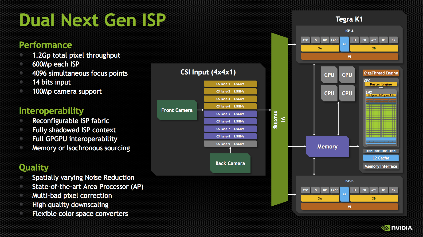
For those not familiar, ISP (Image Signal Processor) handles the imaging pipeline for still photos, video, and performs tasks like Bayer to RGB conversion (demosaicing), 3A (Autofocus, Auto Exposure, Auto white balance), noise reduction, lens correction, and so on. Although NVIDIA has always included an ISP onboard, I couldn’t shake the feeling that still imaging performance could’ve been better, especially in the few cases that allowed direct comparison (HTC One X). With Tegra K1, there’s more die area dedicated to ISP than in the past, and there are two of them to support the kind of dual camera applications that have quickly become popular.
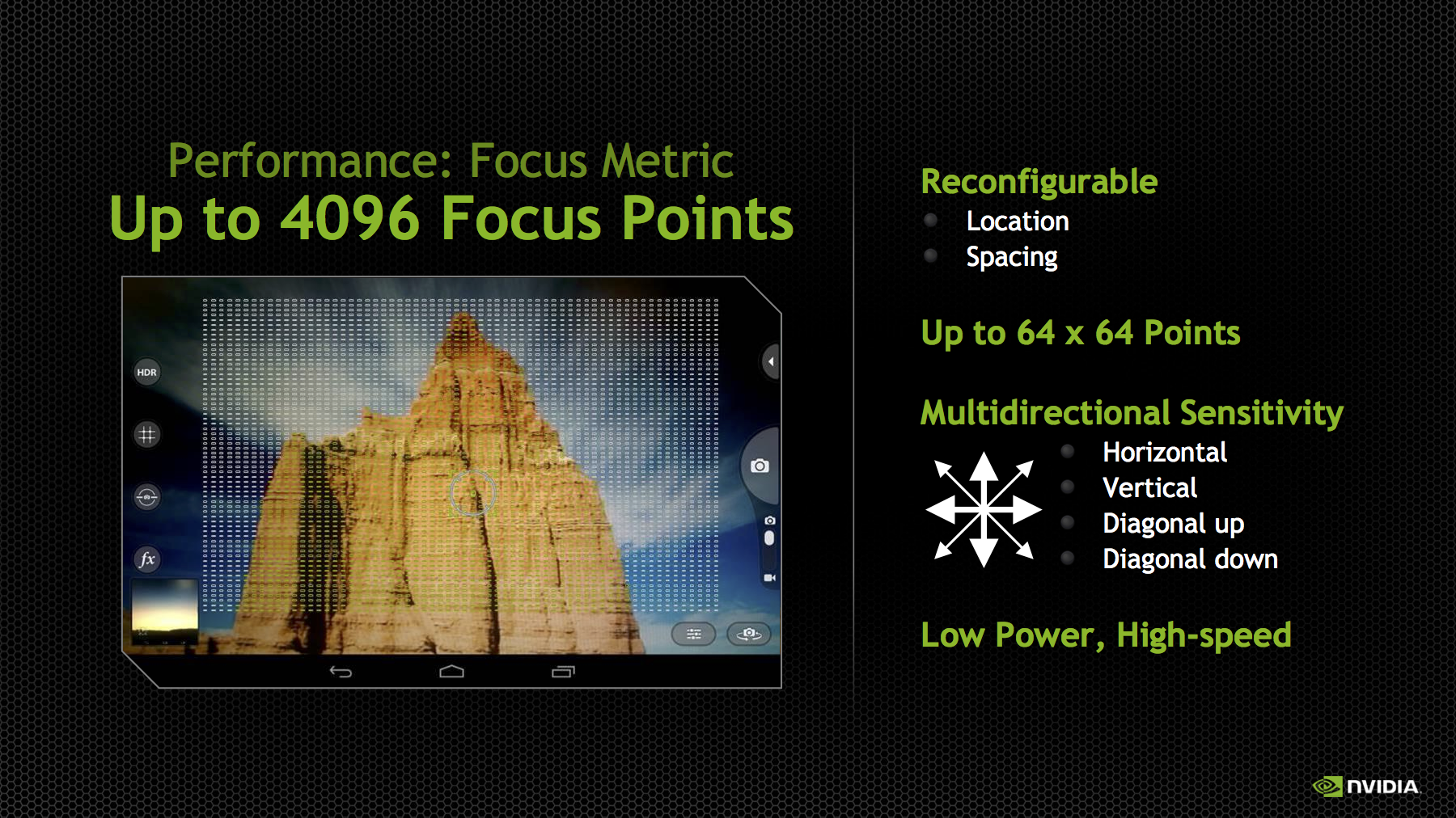
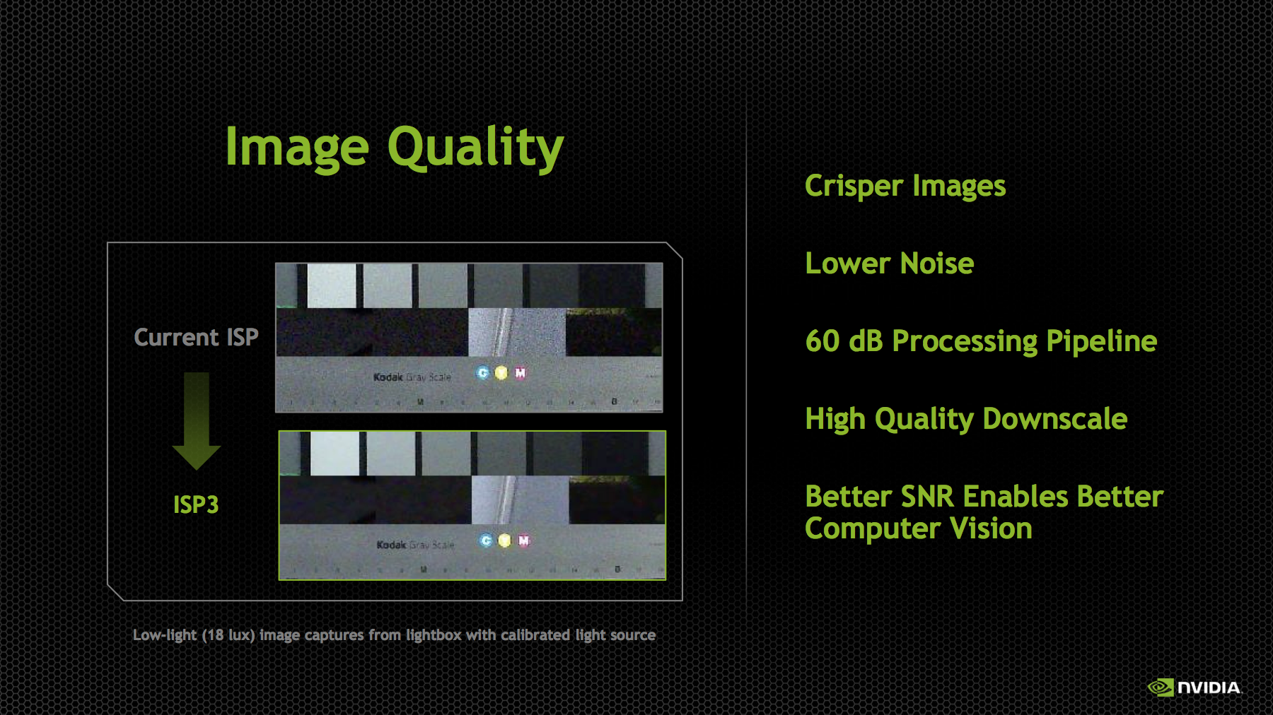
Tegra K1 includes the third generation of NVIDIA’s ISP, capable of processing 600 MP/s on each ISP with 14 bit input, and support for up to 100 MP cameras. There are two of them, so NVIDIA quotes the total pixel throughput as up to 1.2 Gp/s. This is dramatically increased from Tegra 4, which supported up to 400 Mp/s at 10 bits per pixel. In addition the K1’s ISP now supports up to 4096 focus points, a 64x64 array, for its autofocus routine. The ISP also has better noise reduction, and local tone mapping, a feature we’ve also seen become popular for combining parts of images and recovering some of the dynamic range lost with ever shrinking pixel sizes.
Tegra K1 retains compatibility with the Chimera 1.0 features that we just saw in the Tegra Note 7, like object tracking, always-on HDR, slow motion capture, and full resolution burst, and adds more. NVIDIA has kept the Chimera brand for the K1 SoC, calling it Chimera 2.0, and envisions this architecture enabling things like better temporal pixel binning (combining 8 exposures from the CMOS to drive noise down further), faster panorama, video stabilization, and even better live preview with effects applied. The high level of Chimera seems to be the same – kernels that either run on the CPU, or on the GPU (ostensibly in CUDA this time) before or after the ISP and in a variety of image spaces (Bayer or RGB depending).
On the video side, Tegra K1 continues to support 2160p30 (4K or UHD video at 30FPS) encode and decode. Broken down another way, H.264 High Profile Level 5.1 decode and 4K H.264 High Profile 4.2 encode. The fact that there’s a Kepler next door made me suspect that NVENC was used for most of these tasks, but it turns out that NVIDIA still has discrete blocks for video encode of H.264, VP8, VC1, and others. These are the same video encode and decode blocks as what were used in Tegra 4, but with some further optimizations for power and efficiency. The Tegra K1 platform includes support for H.265 video decode as well, but this isn’t accelerated fully in hardware, rather the decode is split across NVENC and CPU.
NVIDIA showed off a K1 reference board doing 4Kp30 H.264 decode on an attached display, I didn’t notice any dropped frames. Of course that’s a given considering we saw the same thing on Tegra 4, but it’s still worth noting that the SoC is capable of driving 4K/UHD displays over eDP 1.4, LVDS and HDMI 1.4b.
The full GPIO breakdown for Tegra K1 includes essentially all the requisite connectivity you’d expect for a mobile SoC. For USB there’s 3 USB 2.0 ports, and 2 USB 3.0 ports. For storage Tegra K1 supports eMMC up to version 4.5.1, and there’s PCIe x4 which can be configured


88 Comments
View All Comments
da_asmodai - Monday, January 6, 2014 - link
This articles says first, first, first for Kepler core in mobile but it's not out yet and I believe everything that's claimed as a first in this article is also supported by the Adreno 420 in the already announced Snapdragon 805. I'd like to see a side by side spec comparison of Kepler, Adreno 420, and PowerVR Series 6XT.dwforbes - Monday, January 6, 2014 - link
"FP64 support is also present, at 1/24 the FP32 rate"Should this 1/2 the FP32 rate, or is it really so crippled?
Ryan Smith - Monday, January 6, 2014 - link
No, 1/24 is correct. It's so that you have native FP64 when you need it, but you aren't wasting die space on precision you aren't going to use.ddriver - Monday, January 6, 2014 - link
nvidia being cheap once again, deliberately ruining compute performance like they did with desktop GPUs for years. And let me guess, no openCL support either? Thanks but no thanks, gonna stick to qualcomm and samsung mobile platforms and amd/radeon on the desktop. And for what? To push their ridiculously and shamelessly overpriced "professional" products?GTX 780 DP @ 1/24 SP
R9 290 DP @ 1/8 SP
R9 280 DP @ 1/4 SP
Loki726 - Monday, January 6, 2014 - link
Adding big double precision units has real area and power costs (you typically can't rail gate off individual functional units). If you put full-rate double precision units in a mobile SoC it would just sit there draining your battery life.ddriver - Monday, January 6, 2014 - link
Unfortunately, power efficiency is just the excuse to deliberately cripple compute performance of consumer products. As you see, AMD has no problem providing DP support with lower penalty, which is the reason my compute farm runs radeons exclusively, because the performance per $ ratio completely destroys prosumer products. I do realize I am a very specific and narrow case, since I couldn't care less about gaming and graphics performance, since I use it only to rasterize the compute output, but still... why not go for a more performing design, considering it is not that much about efficiency but the greed for the fat profit margins of teslas and quadros that motivates nvidia to cripple DP performance to such a horrendous extent.Loki726 - Monday, January 6, 2014 - link
AMD doesn't release a mobile GPU part, and the Qualcomm parts which are based off of the old AMD VLIW5 design that they bought from AMD don't include double precision. Every little bit of power matters in mobile.ddriver - Monday, January 6, 2014 - link
The 1/24 DP performance does not come as a mobile-dedicated design, even the GTX 780 is crippled this way, even though it is an enthusiast part, where power efficiency is the least concern.Loki726 - Monday, January 6, 2014 - link
They are different strategies. Neither one is ideal for everyone.Putting double precision hardware into consumer parts is effectively asking
gamers to pay for extra area and power. I do agree that this is less of an
issue in desktop parts compared to mobile, but it is still an issue and GPUs
have enough ALUs in them that you would notice it if every one of them got 10%
less efficient in benchmarks.
AMD builds one chip and sells it into both compute and graphics markets. In
order to make it appealing for compute applications they add double precision.
They make gamers pay for this even though they never use it, but they don't have
to pay the design costs of building multiple chips. NVIDIA builds two
different designs. One chip for compute and another one for graphics (although
this round they also sold the compute chip into the graphics market - Titan).
Presumably they do this because they think that they can recoup the extra cost
of building a different chip that only compute users buy, and by doing so
they don't make gamers pay extra for double precision.
The compute chip has extra features like more registers, ECC, more double
precision units, dynamic parallelism, etc. Chip design is expensive. Think
hundreds of millions of dollars for a new design. If there were just as many
users of compute GPUs as there are gamers who buy graphics cards, the prices
would probably come down a lot.
I'm with you that I would like to have cheaper compute parts with full double
precision support, but I think the only real way to drive down chip prices is to
make them a commodity. It won't happen until there is a killer compute app
that makes every desktop owner want to go out and buy a compute GPU.
ddriver - Tuesday, January 7, 2014 - link
And how do consumers exactly "pay extra" for the better DP performance when AMD GPUs are overall much better value than nvidia gpus? It seems to me that if the extra cost is as high as you believe it is (which it really isn't) then it is AMD that pays it with its profit margins.