ASUS Maximus VI Impact Review: ROG and Mini-ITX
by Ian Cutress on November 22, 2013 10:00 AM ESTASUS Maximus VI Impact In The Box
In The Box analysis is straightforward: a product that ends up being more expensive than those similar to it must have something extra to provide. While the ASUS Z87 Maximus VI Impact is one of the more expensive mini-ITX boards, it is very hardware rich. Nonetheless, a ROG product, historically speaking, has something a little extra. In the box we get:
User Guide
Rear IO Shield
Driver CD
SupremeFX Impact Video Card
mPCIe Combo II card, with a dual band 802.11ac/BT4.0 WiFi module and M.2 support
WiFi Antenna
Two SATA Cables
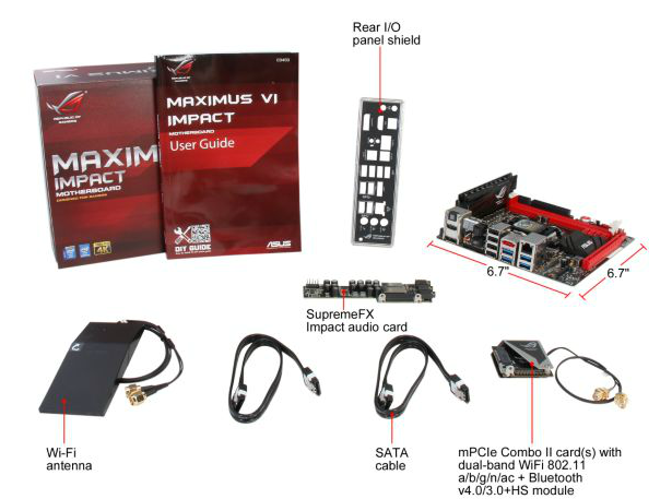
The SupremeFX audio card and mPCIe combo have already been covered in the review, which just leaves the SATA cables and WiFi antenna as the true ‘new’ contents to be discussed. The WiFi antenna is a new design for ASUS, taking the two outputs from the WiFi card and supplying an orthogonal stand to help maximize picking up a WiFi signal. To be honest, I preferred the magnetic loops of the P8Z77-I Deluxe. Also, I would have preferred a full complement of SATA cables: two covers the basics, but SSD + ODD + Storage is not covered here.
ASUS Maximus VI Impact Overclocking
Experience with ASUS Maximus VI Impact
I am not sure whether it is because I have recently been testing mini-ITX boards, whether the onset of winter is lowering ambient temperatures or if my processor is getting better with age: using the M6I, much like the last mITX motherboard I reviewed, we hit 4.7 GHz with the 4770K CPU with peak temperatures under 90C. Earlier in the year, our limit was more around 4.6 GHz, with 4.7 GHz getting very toasty at high voltages. An interesting one that.
In terms of overclocking options, ASUS design every ROG motherboard to be taken to sub-zero temperatures by enthusiasts, thus there are more options than you can shake a stick at in the BIOS. In terms of overclocking options, ASUS’ main plug here is the OS software, using 4-Way Optimization. In the BIOS we get a Gamer’s OC Profile, as well as CPU Level Up from 4.2 GHz to 4.6 GHz using a lookup table of voltages. I would have liked some of these CPU Level Up options in the OS as well, to give users more customizability through the OS.
Methodology:
Our standard overclocking methodology is as follows. We select the automatic overclock options and test for stability with PovRay and OCCT to simulate high-end workloads. These stability tests aim to catch any immediate causes for memory or CPU errors.
For manual overclocks, based on the information gathered from previous testing, starts off at a nominal voltage and CPU multiplier, and the multiplier is increased until the stability tests are failed. The CPU voltage is increased gradually until the stability tests are passed, and the process repeated until the motherboard reduces the multiplier automatically (due to safety protocol) or the CPU temperature reaches a stupidly high level (100ºC+). Our test bed is not in a case, which should push overclocks higher with fresher (cooler) air.
Automatic Overclock:
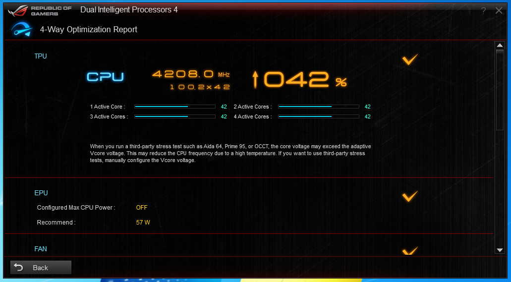
The first at most obvious place for an automatic overclock is the OS, where we use the 4-Way Optimization in AI Suite, as shown to the left here:
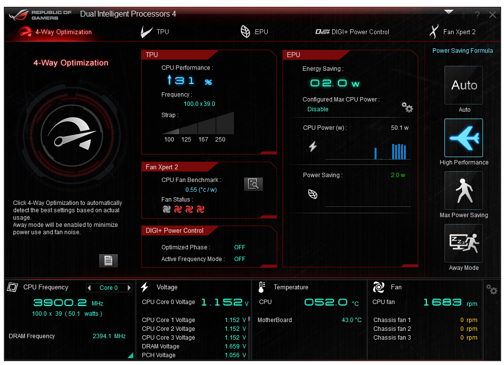
With the 4WO setting, the system applied a 42x100.2 overclock (4208 MHz), with a CPU voltage of 1.150 volts. This lead to a load voltage of 1.168 volts, a peak OCCT temperature of 68C and a PovRay score of 1727.59.
In the BIOS, we get four main options. The first is the Gamer’s OC Profile, and then three CPU Level Up options from 4.2 GHz to 4.6 GHz in 200 MHz jumps.

On the Gamer’s OC Profile, the system set the CPU multiplier staggered from 47x to 44x depending on loading. For this, the CPU was set to 1.250 volts and XMP applied. In the OS, this led to a PovRay score of 1803.03, but the system BSODed on OCCT as our CPU cannot handle 4.7 GHz at this voltage.
On the first CPU Level Up option, the system is set to 4.2 GHz with 1.250 volts on the CPU. In the OS, this led to a load voltage of 1.264 volts, a peak OCCT temperature of 77C and a PovRay score of 1741.59.
For CPU Level Up 2, the system is set to 4.4 GHz with 1.250 volts on the CPU. In the OS, this led to a load voltage of 1.264 volts, a peak OCCT temperature of 78C and a PovRay score of 1823.56.
For CPU Level Up 3, the system is set to 4.6 GHz with 1.250 volts on the CPU. In the OS, this led to a load voltage of 1.264 volts, a PovRay score of 1900.2 but would BSOD during OCCT.
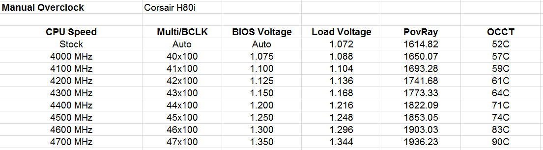
Manual Overclock:
For our manual overclock, we start at 40x100 with 1.000 volts on the CPU, and work our way up: when stable the multiplier is increased, and when unstable the voltage is increased. For the M6I the CPU Load Line calibration was set to Level 7, one below maximum.


69 Comments
View All Comments
Morawka - Saturday, November 23, 2013 - link
it's ATA Secure. Every nand chip in the ssd gets cleared out by writing zeroes to the entire drive.Gigaplex - Monday, November 25, 2013 - link
That's not necessarily how it works, especially for SandForce based controllers.colinisation - Friday, November 22, 2013 - link
Could you test out an M2 SSD in the MPCie Combo card slot, I am interested to see if it chokes the SSD?Mr Perfect - Friday, November 22, 2013 - link
Two questions about the overview on page one.First, what is the difference between using the FastBoot jumper to toggle between UEFI booting methodology and the legacy boot sequence? Under what circumstances would you want to use an older, slower boot method?
Second, the top right button on the "Impact Control" board is labeled as Clear CMOS, but the paragraph under the picture describes it as a USB BIOS Flashback button. Is this a dual function button, or am I missing something?
DanNeely - Friday, November 22, 2013 - link
Using an obsolete OS *cough*Windows XP*cough* that doesn't support UEFI would be an obvious example.Some people in OSS land have a massive hateon for UEFI because it's much more heavily controlled and patent encumbered by Intel and might refuse to use it for ideological reasons.
Morawka - Saturday, November 23, 2013 - link
First: When Using Liquid Nitrogen to OverclockSecond: No it's a error. USB Bios Flashback button is found on the i/O shield and the usb stick must be in the designated port.
Mr Perfect - Monday, November 25, 2013 - link
Hmm, okay, thanks.martixy - Friday, November 22, 2013 - link
That moment when you discover a whole new dimension just waiting for you to play in!creed3020 - Friday, November 22, 2013 - link
Thanks so much for the review Ian! I have been waiting for this review since the ASUS Z87 lineup launched. I was floored that a mini-ITX board was joining the ROG lineup. I'm hoping for my new build to be centered around this board.Arbie - Friday, November 22, 2013 - link
It's simply amazing that one can buy this much engineering, fabrication, and quality for $225.