Intel’s Silvermont Architecture Revealed: Getting Serious About Mobile
by Anand Lal Shimpi on May 6, 2013 1:00 PM EST- Posted in
- CPUs
- Intel
- Silvermont
- SoCs
The Silvermont Module and Caches
Like AMD’s Bobcat and Jaguar designs, Silvermont is modular. The default Silvermont building block is a two-core/two-thread design. Each core is equally capable and there’s no shared execution hardware. Silvermont supports up to 8-core configurations by placing multiple modules in an SoC.
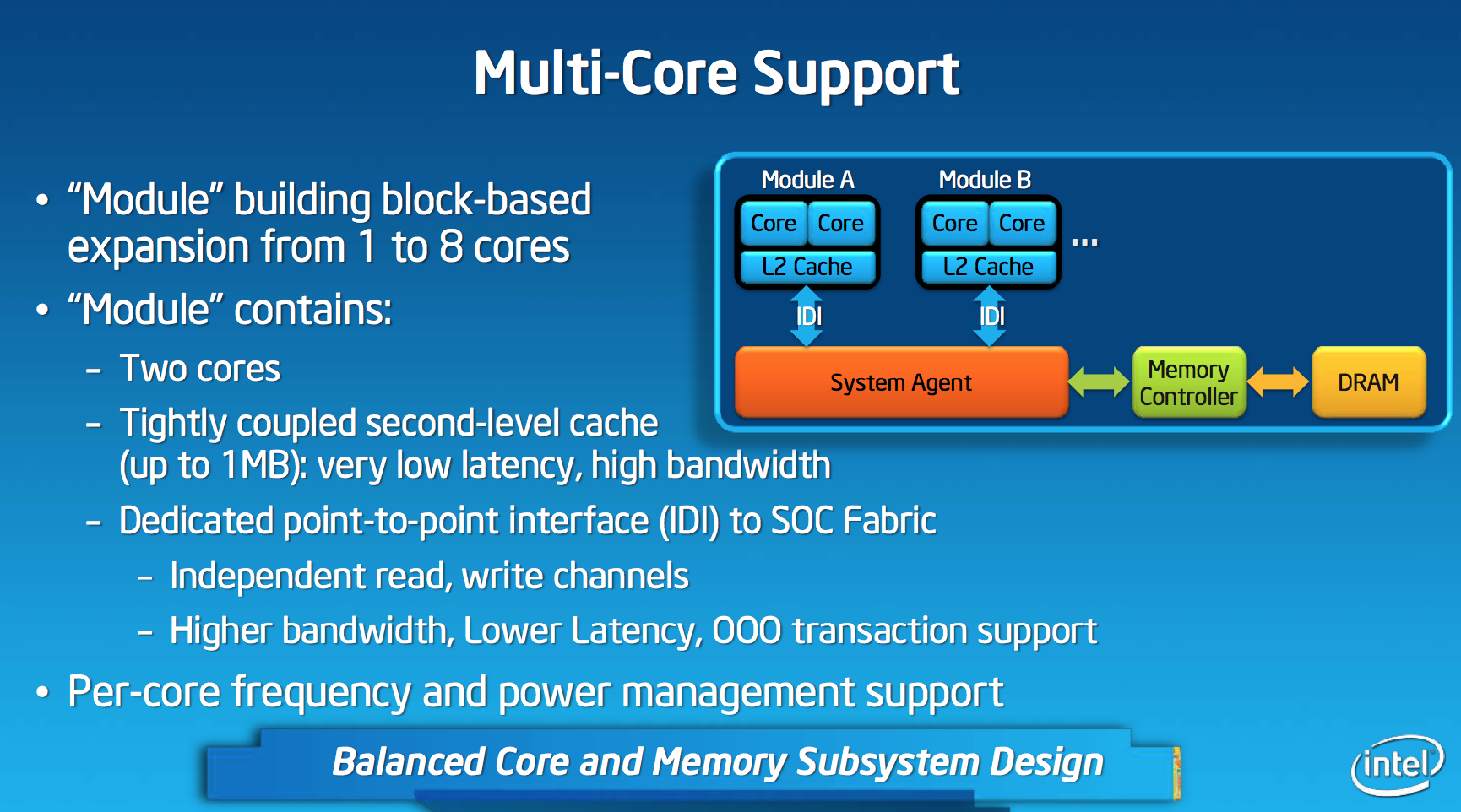
Each module features a shared 1MB L2 cache, a 2x increase over the core:cache ratio of existing Atom based processors. Despite the larger L2, access latency is reduced by 2 clocks. The default module size gives you clear indication as to where Intel saw Silvermont being most useful. At the time of its inception, I doubt Intel anticipated such a quick shift to quad-core smartphones otherwise it might’ve considered a larger default module size.
L1 cache sizes/latencies haven’t changed. Each Silvermont core features a 32KB L1 data cache and 24KB L1 instruction cache.
Silvermont Supports Independent Core Frequencies: Vindication for Qualcomm?
In all Intel Core based microprocessors, all cores are tied to the same frequency - those that aren’t in use are simply shut off (power gated) to save power. Qualcomm’s multi-core architecture has always supported independent frequency planes for all CPUs in the SoC, something that Intel has always insisted was a bad idea. In a strange turn of events, Intel joins Qualcomm in offering the ability to run each core in a Silvermont module at its own independent frequency. You could have one Silvermont core running at 2.4GHz and another one running at 1.2GHz. Unlike Qualcomm’s implementation, Silvermont’s independent frequency planes are optional. In a split frequency case, the shared L2 cache always runs at the higher of the two frequencies. Intel believes the flexibility might be useful in some low cost Silvermont implementations where the OS actively uses core pinning to keep threads parked on specific cores. I doubt we’ll see this on most tablet or smartphone implementations of the design.
From FSB to IDI
Atom and all of its derivatives have a nasty secret: they never really got any latency benefits from integrating a memory controller on die. The first implementation of Atom was a 3-chip solution, with the memory controller contained within the North Bridge. The CPU talked to the North Bridge via a low power Front Side Bus implementation. This setup should sound familiar to anyone who remembers Intel architectures from the late 90s up to the mid 2000s. In pursuit of integration, Intel eventually brought the memory controller and graphics onto a single die. Historically, bringing the memory controller onto the same die as the CPU came with a nice reduction in access latency - unfortunately Atom never enjoyed this. The reasoning? Atom never ditched the FSB interface.
Even though Atom integrated a memory controller, the design logically looked like it did before. Integration only saved Intel space and power, it never granted it any performance. I suspect Intel did this to keep costs down. I noticed the problem years ago but completely forgot about it since it’s been so long. Thankfully, with Silvermont the FSB interface is completely gone.
Silvermont instead integrates the same in-die interconnect (IDI) that is used in the big Core based processors. Intel’s IDI is a lightweight point to point interface that’s far lower overhead than the old FSB architecture. The move to IDI and the changes to the system fabric are enough to improve single threaded performance by low double digits. The gains are even bigger in heavily threaded scenarios.
Another benefit of moving away from a very old FSB to IDI is increased flexibility in how Silvermont can clock up/down. Previously there were fixed FSB:CPU ratios that had to be maintained at all times, which meant the FSB had to be lowered significantly when the CPU was running at very low frequencies. In Silvermont, the IDI and CPU frequencies are largely decoupled - enabling good bandwidth out of the cores even at low frequency levels.
The System Agent
Silvermont gains an updated system agent (read: North Bridge) that’s much better at allowing access to main memory. In all previous generation Atom architectures, virtually all memory accesses had to happen in-order (Clover Trail had some minor OoO improvements here). Silvermont’s system agent now allows reordering of memory requests coming in from all consumers/producers (e.g. CPU cores, GPU, etc...) to optimize for performance and quality of service (e.g. ensuring graphics demands on memory can regularly pre-empt CPU requests when necessary).


174 Comments
View All Comments
R0H1T - Tuesday, May 7, 2013 - link
Let's see, umm Snapdragon 600 & then there's this soon to be released 800 ? So lemme get this straight, an unreleased product vs one that was available last year, Intel's latest(future indefinite) vs old/dated(relatively) from ARM seems fair to me !ssiu - Monday, May 6, 2013 - link
Exactly the 2 points I wonder about too:(1) GPU performance -- 1/4 of an HD4000, about iPad 4 level -- so slower than e.g. PowerVR Rogue which should come out around the same time
(2) more importantly, even if Intel can make competitive/superior product, can it survive on such low margin?
zeo - Wednesday, May 8, 2013 - link
Well, yes and no on point 1... The iPad is using a quad SGX544, and Rogue doesn't improve performance by that massive amount that a single Rogue/Series 6 could beat a quad Series 5. So it's not that Rogue will be better than the Bay Trail GMA but can scale higher with a multiple configuration!On the margins, Intel is lowering their costs moving to 22nm FAB and despite the declining PC market they're still doing well and so should be fine for the foreseeable future... They'll have to do terribly in all markets to really start hurting now and that's not likely yet...
andrewaggb - Monday, May 6, 2013 - link
too early to say I think. This atom should be pretty good. if it's both twice as fast as the old atom and uses less power (which I believe is what they are trying to tell us), that's pretty good. It will be competing with 2nd gen a-15 designs or better, so the current performance claims are largely meaningless. GPU performance continues to be an issue, aiming for last years performance is definitely way too low. Fortunately gpu speed can normally be scaled more quickly than cpu speed, but intel seems to consistently underspec on gpu so I doubt they'll do better this time. Unless they go haswell style and have various different gpu skus. guess we'll see.Considering how much success rambus has had suing everybody I think if intel wanted to they could probably sue anybody working on advanced processor designs without sufficient licensing arrangements. Drive the minimum cost up a bit so the margins are higher.
R0H1T - Tuesday, May 7, 2013 - link
This comment is hilarious ~ "gpu speed can normally be scaled more quickly than cpu speed" that's only if you're packing moar cores i.e. like SNB<IVB<<Haswell !GPU's cannot be scaled for performance unless there's some major redesigns of the underlying architecture, like AMD's transition to GCN, so unless you've got some insider info into how Intel plans to use their superior Iris(Pro) graphics in Silvermont I see this myth, about Intel's superior graphics, of yours being busted yet again, only this time in the mobile arena !
ominobianco - Monday, May 6, 2013 - link
If you had actually read the article you would know that they are comparing against performance PROJECTIONS of competitors parts available at product launch time, NOT current parts.zeo - Wednesday, May 8, 2013 - link
Sorry but ARMv8 64bit aren't coming out till the later half of 2014 at the earliest and they're pushing to be on 16nm and not 20nm, which may delay them further!While there's no major improvements planned for ARM until then! Many of the original Cortex A15 SoC releases have been delayed from 2012 to 2013!
MrSpadge - Monday, May 6, 2013 - link
Error: On page 1 you correctly write "Remember that power scales with the square of voltage". Almost immediately followed by "At 1V, Intel’s 22nm process gives ... or at the same performance Intel can run the transistors at 0.8V - a 20% power savings."Ouch - forgot that square!
dusk007 - Monday, May 6, 2013 - link
I thought we would wait for 14nm for Intel to definitely pull ahead. This looks very promising.Now my perfect smartphone would sport a dual core Silvermont with a 4000mah battery, the HTC One camera and otherwise durable.
GPU I don't care as long as it is good enough for the GUI I don't play games that would require something fast. Thin? Not at the cost of a smaller battery.
I would love some feature phone like battery life. Triple what we have to deal with now would be incredible and possible it seems to me. Maybe the Motorola Phone X x86 Version can deliver that.
Camera is secondary and I don't need a 1080p screen. Just 4.3-4.5" of 720p and long battery life.
I feel like battery life is where this new generation can really promise new things. 32nm Atom already does really well in the tablets compared to quad core ARM competition. It will be a waste if they add 1500mah batteries though. I hope they finally realize as smartphones are mainstream that a lot of people would care first about battery life and second about 7mm thinness.
beginner99 - Tuesday, May 7, 2013 - link
Agree. Current phones are too big, 1080p is pretty much useless and wastes battery life and even the GPU in Medfield is good enough for the GUI. The lower screen resolution of course helps too with needing a not so good GPU. But with both you save on power. I want a phone I need to charge once a week not every day.