Intel’s Silvermont Architecture Revealed: Getting Serious About Mobile
by Anand Lal Shimpi on May 6, 2013 1:00 PM EST- Posted in
- CPUs
- Intel
- Silvermont
- SoCs
OoOE
You’re going to come across the phrase out-of-order execution (OoOE) a lot here, so let’s go through a quick refresher on what that is and why it matters.
At a high level, the role of a CPU is to read instructions from whatever program it’s running, determine what they’re telling the machine to do, execute them and write the result back out to memory.
The program counter within a CPU points to the address in memory of the next instruction to be executed. The CPU’s fetch logic grabs instructions in order. Those instructions are decoded into an internally understood format (a single architectural instruction sometimes decodes into multiple smaller instructions). Once decoded, all necessary operands are fetched from memory (if they’re not already in local registers) and the combination of instruction + operands are issued for execution. The results are committed to memory (registers/cache/DRAM) and it’s on to the next one.
In-order architectures complete this pipeline in order, from start to finish. The obvious problem is that many steps within the pipeline are dependent on having the right operands immediately available. For a number of reasons, this isn’t always possible. Operands could depend on other earlier instructions that may not have finished executing, or they might be located in main memory - hundreds of cycles away from the CPU. In these cases, a bubble is inserted into the processor’s pipeline and the machine’s overall efficiency drops as no work is being done until those operands are available.
Out-of-order architectures attempt to fix this problem by allowing independent instructions to execute ahead of others that are stalled waiting for data. In both cases instructions are fetched and retired in-order, but in an OoO architecture instructions can be executed out-of-order to improve overall utilization of execution resources.
The move to an OoO paradigm generally comes with penalties to die area and power consumption, which is one reason the earliest mobile CPU architectures were in-order designs. The ARM11, ARM’s Cortex A8, Intel’s original Atom (Bonnell) and Qualcomm’s Scorpion core were all in-order. As performance demands continued to go up and with new, smaller/lower power transistors, all of the players here started introducing OoO variants of their architectures. Although often referred to as out of order designs, ARM’s Cortex A9 and Qualcomm’s Krait 200/300 are mildly OoO compared to Cortex A15. Intel’s Silvermont joins the ranks of the Cortex A15 as a fully out of order design by modern day standards. The move to OoO alone should be good for around a 30% increase in single threaded performance vs. Bonnell.
Pipeline
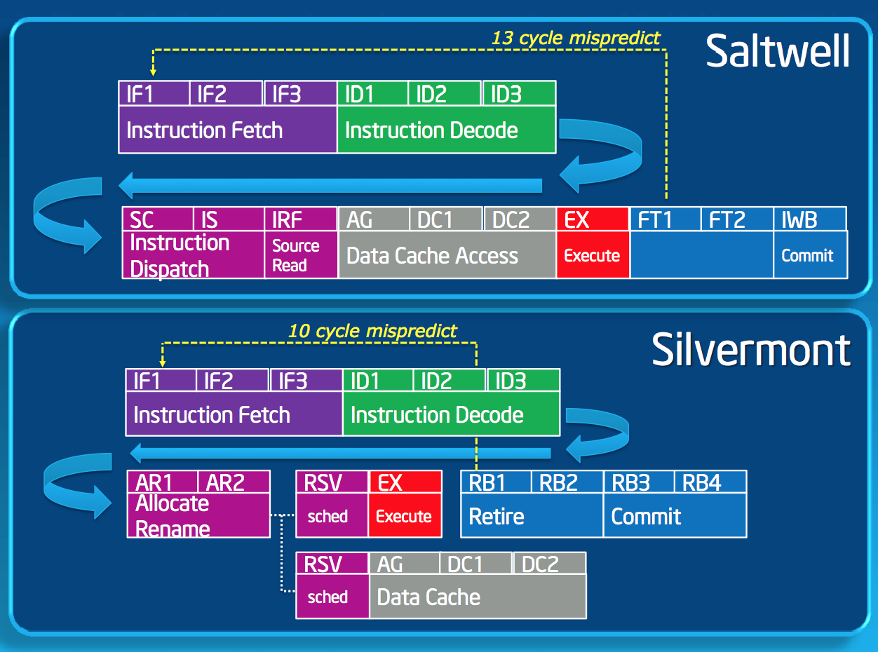
Silvermont changes the Atom pipeline slightly. Bonnell featured a 16 stage in-order pipeline. One side effect to the design was that all operations, including those that didn’t have cache accesses (e.g. operations whose operands were in registers), had to go through three data cache access stages even though nothing happened during those stages. In going out-of-order, Silvermont allows instructions to bypass those stages if they don’t need data from memory, effectively shortening the mispredict penalty from 13 stages down to 10. The integer pipeline depth now varies depending on the type of instruction, but you’re looking at a range of 14 - 17 stages.
Branch prediction improves tremendously with Silvermont, a staple of any progressive microprocessor architecture. Silvermont takes the gshare branch predictor of Bonnell and significantly increased the size of all associated data structures. Silvermont also added an indirect branch predictor. The combination of the larger predictors and the new indirect predictor should increase branch prediction accuracy.
Couple better branch prediction with a lower mispredict latency and you’re talking about another 5 - 10% increase in IPC over Bonnell.


174 Comments
View All Comments
xTRICKYxx - Tuesday, May 7, 2013 - link
You're right. Intel has nothing to show at all.... Its not like they have the most powerful mobile and desktop consumer processors available.R0H1T - Tuesday, May 7, 2013 - link
Yeah, now sit & watch that market(x86) die a slow death at the hands of mobile/tablets that are powered by "good enough" ARM which doesn't need teraflop level of performance to sell their stuff unlike Intel !misaki - Monday, May 6, 2013 - link
Wow, clearly you are a new reader. This is an architecture overview, not a performance article, which means the information HAS to come from Intel. They have done these type of articles with every architecture redesign since the 90's.When chips are available to test that is when the real world performance articles will come out.
Ortanon - Monday, May 6, 2013 - link
SERIOUSLY.kyuu - Monday, May 6, 2013 - link
Yes, but a lot of performance claims are being made in the article, and Anand really seemed to just be taking Intel's marketing speak for gospel. That's how it read, at least.xTRICKYxx - Tuesday, May 7, 2013 - link
Not really. He clearly states to take the graphs cautiously. Also Intel may be slightly misleading, but nothing in the graphs are lies. They chose the best possible scenario for the greatest advantage.R0H1T - Tuesday, May 7, 2013 - link
Like how they(AT) claimed Intel's "SDP" was superior after stress testing an Exynos Octa, yup loved that fairytale !Kevin G - Monday, May 6, 2013 - link
The article mentions that the IDI is similar to internal bus found on the Nehalem and later desktop processor. IDI here is mentioned as a point-to-point interconnect where as everything is linked via a ring bus in recent Core processors. Of course you can loop multipe point-to-point interfaces into a loop but the article's wording allows for other topologies.For example, each Silvermont module could have its down dedicated point-to-point link to the system agent. In Nehalem, the system against logically appears as another hop in the internal ring bus.
Exophase - Monday, May 6, 2013 - link
Small correction:"Remember that with the first version of Atom, Intel enabled the fusion of load-op-store and load-op-execute instructions. Instead of these instruction combinations decoding into three and two micro-ops respectively, they would be fused post-fetch and treated like single operations throughout the entire pipeline."
Atom (the current one anyway) doesn't have instruction (macro-op) fusion. It does handle load + op and load + op + store are one issue down the pipeline but they still came from single instructions that are a natural part of the x86 ISA. While these may be considered fused micro-ops in Intel's other CPUs that terminology doesn't fit Atom.
These operations do need multiple instructions on most more RISCy ISAs like ARM. But the same is true the other way around (notably, 3 address arithmetic). I very much doubt you'll find typical x86 programs only need 2 instructions for every 3 ARM instructions on average, or at least any papers I've seen that measure micro-ops vs instructions on high-end CPUs are nowhere close to 1.5 (and a uop isn't generally more powerful than an ARM instruction, sometimes less when you consider two are needed for a store). But there are lots of other places that caused stalls on Atom that weren't related to decode, that it's easy to see how you could still gain a lot of perf/MHz without increasing it - as Bobcat and Jaguar have shown. All the details here do seem to point to a Bobcat-like design only with a much lower L2 cache latency and branch mispredict penalty which can only help more.
Anand Lal Shimpi - Monday, May 6, 2013 - link
Er you're very correct. Atom doesn't break these instructions down further, they're treated like single ops throughout the pipeline. I've updated the section. Thank you!