NVIDIA's Tegra 3 Launched: Architecture Revealed
by Anand Lal Shimpi on November 9, 2011 12:34 AM ESTThe Tegra 3 GPU: 2x Pixel Shader Hardware of Tegra 2
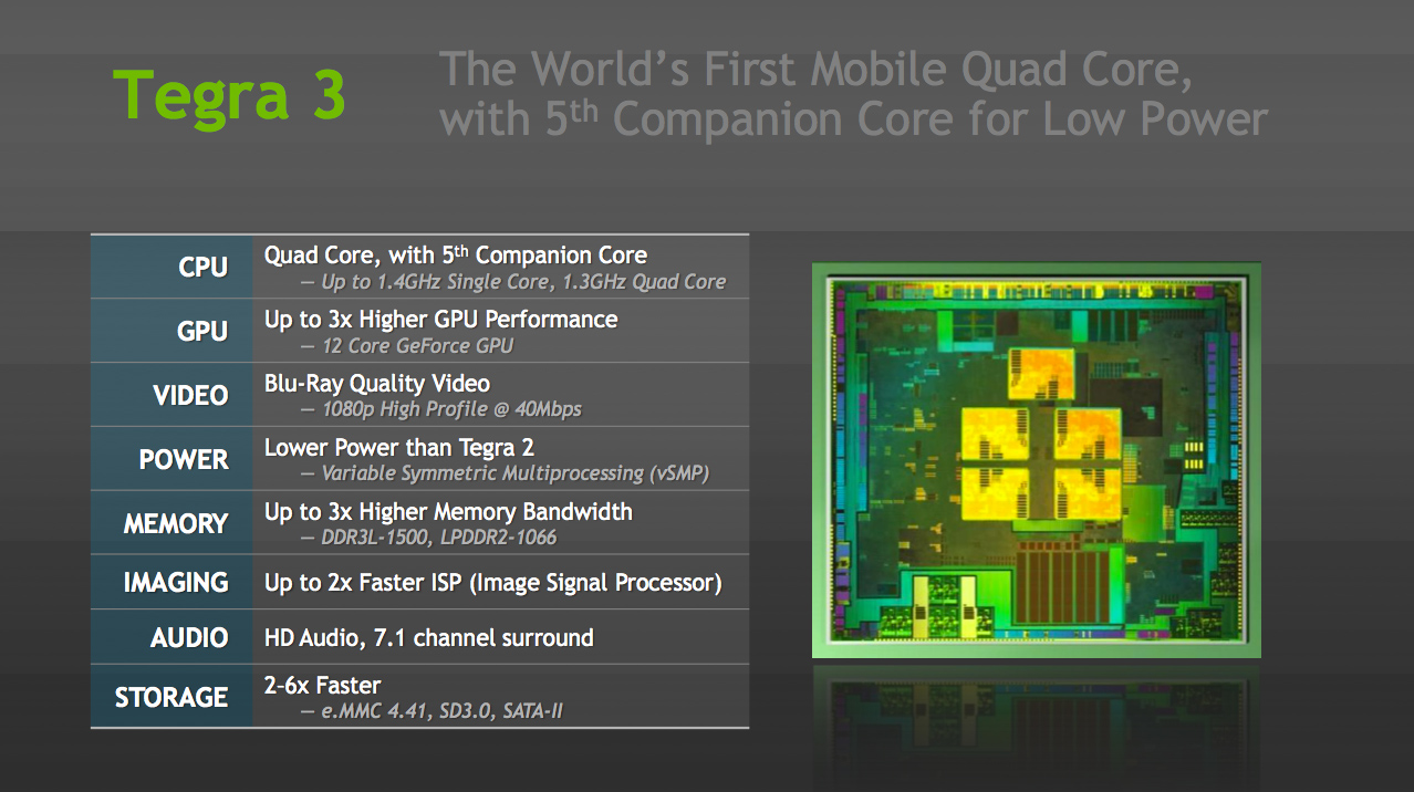
Tegra 3's GPU is very much an evolution of what we saw in Tegra 2. The GeForce in Tegra 2 featured four pixel shader units and four vertex shader units; in Tegra 3 the number of pixel shader units doubles while the vertex processors remain unchanged. This brings Tegra 3's GPU core count up to 12. NVIDIA still hasn't embraced a unified architecture, but given how closely it's mimicking the evolution of its PC GPUs I wouldn't expect such a move until the next-gen architecture - possibly in Wayne.
| Mobile SoC GPU Comparison | |||||||||||
| Adreno 225 | PowerVR SGX 540 | PowerVR SGX 543 | PowerVR SGX 543MP2 | Mali-400 MP4 | GeForce ULP | Kal-El GeForce | |||||
| SIMD Name | - | USSE | USSE2 | USSE2 | Core | Core | Core | ||||
| # of SIMDs | 8 | 4 | 4 | 8 | 4 + 1 | 8 | 12 | ||||
| MADs per SIMD | 4 | 2 | 4 | 4 | 4 / 2 | 1 | 1 | ||||
| Total MADs | 32 | 8 | 16 | 32 | 18 | 8 | 12 | ||||
| GFLOPS @ 200MHz | 12.8 GFLOPS | 3.2 GFLOPS | 6.4 GFLOPS | 12.8 GFLOPS | 7.2 GFLOPS | 3.2 GFLOPS | 4.8 GFLOPS | ||||
| GFLOPS @ 300MHz | 19.2 GFLOPS | 4.8 GFLOPS | 9.6 GFLOPS | 19.2 GFLOPS | 10.8 GFLOPS | 4.8 GFLOPS | 7.2 GFLOPS | ||||
Per core performance has improved a bit. NVIDIA worked on timing of critical paths through the GPU's execution units to help it run at higher clock speeds. NVIDIA wouldn't confirm the target clock for Tegra 3's GPU other than to say it was higher than Tegra 2's 300MHz. Peak floating point throughput per core is unchanged (one MAD per clock), but each core should be more efficient thanks to larger caches in the design.
A combination of these improvements as well as newer drivers are what give Tegra 3's GPU its 2x - 3x performance advantage over Tegra 2 despite only a 50% increase in overall execution resources. In pixel shader bound scenarios, there's an effective doubling of execution horsepower so the 2x gains are more believable there. I don't expect many games will be vertex processing bound so the lack of significant improvement there shouldn't be a big issue for Tegra 3.
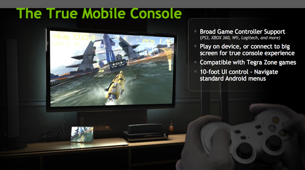
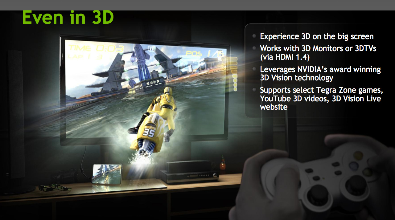
Ready for Gaming: Stereoscopic 3D and Expanded Controller Support
Tegra 3 now supports stereoscopic 3D for displaying content from YouTube, NVIDIA's own 3D Vision Live website and some Tegra Zone games. In its port of Android, NVIDIA has also added expanded controller support for PS3, Xbox 360 and Wii controllers among others.
Tegra 3 Video Encoding/Decoding and ISP
There's unfortunately not too much to go on here, especially not until we have some testable hardware in hand, but NVIDIA is claiming a much improved video decoder and more efficient video encoder in Tegra 3.
Tegra 3's video decoder can accelerate 1080p H.264 high profile content at up to 40Mbps, although device vendors can impose their own bitrate caps and file limitations on the silicon. NVIDIA wouldn't go into greater detail as to what's changed since Tegra 2, other than to say that the video decoder is more efficient. The video encoder is capable of 1080p H.264 base profile encode at 30 fps.
The Image Signal Processor (ISP) in Tegra 3 is twice as fast as what was in Tegra 2 and NVIDIA promised more details would be forthcoming (likely alongside the first Tegra 3 smartphone announcements).
Memory Interface: Still Single Channel, DDR3L-1500 Supported
Tegra 3 supports higher frequency memories than Tegra 2 did, but the memory controller itself is mostly unchanged from the previous design. While Tegra 2 supported LPDDR2 at data rates of up to 600MHz, Tegra 3 increases that to LPDDR2-1066 and DDR3-L is supported at data rates of up to 1500MHz. The memory interface is still only 32-bits wide, resulting in far less theoretical bandwidth than Apple's A5, Samsung's Exynos 4210, TI's OMAP 4, or Qualcomm's upcoming MSM8960. This is particularly concerning given the increase in core count as well as GPU execution resources. NVIDIA doesn't expect memory bandwidth to be a limitation, but I can't see how that wouldn't be the case in 3D games. Perhaps it's a good thing that Infinity Blade doesn't yet exist for Android.
SATA II Controller: On Die
Given Tegra 3 will find itself in convertible Windows 8 tablets, this next feature makes a lot of sense. NVIDIA's latest SoC includes an on-die SATA II controller, a feature that wasn't present on Tegra 2.


94 Comments
View All Comments
psychobriggsy - Friday, November 11, 2011 - link
In the Android market, it really doesn't matter what features Apple includes in their in-house SoC for their iOS devices.Considering that manufacturers are having problems fabbing larger high-DPI displays, I also wouldn't be betting on the iPad 3 having a higher resolution display. And Apple would go for 2048x1536 for simplicities sake.
Five months is also a long time in the ARM SoC market, one that NVIDIA will try to make use of. Let's just hope the product meets the hype when reviews roll in.
name99 - Wednesday, November 9, 2011 - link
I've asked this before, and I will ask it again:What software on Android, shipping TODAY, is capable of using 4 cores usefully?
The browser? The PDF viewer? Google Earth? If so, they're all ahead of their desktop cousins.
Yes, yes, people are buying the future. And, sure, one day, software will be revved to use 4 cores. (But, this being Android, chances are, the particular device you buy this year using Tegra3 will NOT be revved.)
I'm not trying to be snarky here, just realistic. It seems to me the competitors ARM manufacturers are targeting the real world, where dual cores can (to some extent) usefully be used. But nVidia is requiring people who adopt this chip to pay for power that, realistically, they're not going to use. This seems a foolish design choice. It seems to me far more sensible for mobile to basically track (lagging by about a year) desktop. Desktop is seeing quad-core adoption in a few places, but it's hardly mainstream --- and I'd say that until, let's say, the low-end MacBook Air is using quad core, that's an indication that "software" (as a general class) probably hasn't been threaded enough to make quad-core worth-while in mobile.
Yes, it's harder, but until then, I'd say far more useful to look at what's ACTUALLY causing people slowness and hassle on phones and tablets, and add THAT to your chips. So, faster single-threaded core --- great. But think more generally.
Flash on these devices is still slow. Could you speed it up somehow --- maybe a compression engine to transparently compress data sent to/from flash? Likewise app launch is slow. Are there instructions that could be added to speed up dynamic linking? Memory is a problem, and again transparent compression might be helpful there.
Basically --- solve the problems people actually have, even if they are hard, NOT the problems you wish people had because you know how to solve those.
psychobriggsy - Friday, November 11, 2011 - link
The video shows web browsing and games to be using three cores quite often, and the fourth quite a bit. Android is quite multi-threaded, and if it also supports the Java Concurrency APIs it is very easy for software to also be multi-threaded.I also presume that the GeForce drivers and other Tegra SoC drivers utilise multi-threading as much as possible.
And Flash is being dropped on mobile devices in favour of HTML5. That's Adobe making that move. And not before time, it is a horrible technology.
Romulous - Thursday, November 10, 2011 - link
Meh. There may come a time when cores dont metter much.http://www.euclideon.com/ :)
alphadon - Thursday, November 10, 2011 - link
"Die size has almost doubled from 49mm^2 to somewhere in the 80mm^2 range"49^2 = 2401
80^2 = 6400
This should probably read:
"Die size has bloated to over 2.5 times the area of the prior generation leaving everyone wondering why NVIDIA is releasing this 40nm dinosaur. We would have expected a die shrink to keep the power and space requirements in line with the industry's competitors, but seeing all that real estate squandered on such an evolutionary product is downright shameful."
Lugaidster - Friday, November 11, 2011 - link
Did you even read the other posts? The other competitors have bigger dies and less cores! and also, the geometry didn't change between tegra 2 and this.I find it great that they were able to double the shader core count, increase core count from 2 to 5 (it's slower but not less complex, see the die picture) and increase frequency while still having a smaller die than the competition.
I think that given the constraints, this might turn out to be a good product. Obviously only time will tell if it actually performs, but who knows...
Lugaidster - Friday, November 11, 2011 - link
By the way, its 49 mm² not 49² mm. So its actually less than twice as big.psychobriggsy - Friday, November 11, 2011 - link
Do you seriously think the Tegra 3 die size is 8cm by 8cm?49mm^2 is the area, not the edge dimension. In effect the die size has gone from around 7mm x 7mm to 9mm x 9mm. I.e., your little finger nail to your index finger nail (your hands may vary).
psychobriggsy - Friday, November 11, 2011 - link
In addition the 28nm shrink of Tegra 3 (Tegra 3+) next year, if no extra features are added, will shrink the die from 80mm^2 to 40mm^2 (in an ideal world, let's say 50mm^2 worst case and shrinks aren't simple). And Tegra 4 will probably be around 80-100 mm^2 again.lightshapers - Friday, November 11, 2011 - link
This quad core architecture is still disappointing. Actually they implemented a 4th core with good reinforcement from marketing, presented to be a solution for low power consumption at low CPU load. My guess is actually all competitors can do this (cut clocks and power on all but one CPU and reduce cluster frequency) on the ARM dual cluster without the need to add an extra CPU ( I speak for Samsung and TI, as Qualcomm is designing their own). In addition to that, this 5th core is another non negligible additional gates that leak.Then, the action to synchronize L2 Cache by arm coherency port is fast, but 1MB is 1MB, which means probably few hundreds of us for lost reactivity when switching between cluster and this 5th core.
And at the end, it doesn't really solve all the problems of having 4 cores, as asymmetry in core load balance will ever happen. This solution may solve the low load case. But over the low-load watermark, the cluster is power-up, and we have 4 core consuming at least their leakage. This was reported as an issue on tegra2, I don't think it has changed (the 5th is in some way the proof), but here we have 2 additional cores...
For example, medium load requires 2 cores. 5th is off, but consumption is 4 times the consumption of one.
It would have been smarter to design a full speed additional core, so as to get a higher "low limit load" so as to stay on 1st core as longer as possible. With 500Mhz, it's difficult to say if you can manage all graphical interface + OS background on a 720p device...