ARM's Cortex A7: Bringing Cheaper Dual-Core & More Power Efficient High-End Devices
by Anand Lal Shimpi on October 19, 2011 12:31 PM EST- Posted in
- SoCs
- CPUs
- Arm
- Cortex A15
- Smartphones
- Mobile
- Cortex A7
- Tablets
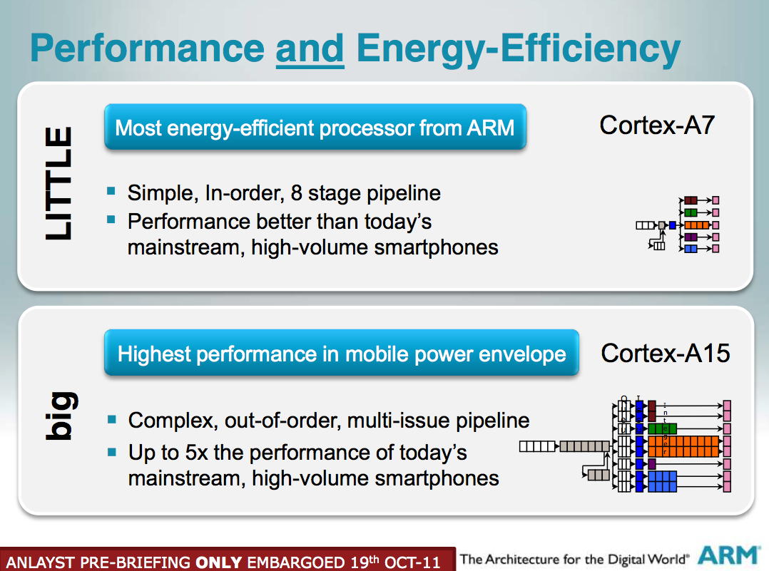
How do you keep increasing performance in a power constrained environment like a smartphone without decreasing battery life? You can design more efficient microarchitectures, but at some point you’ll run out of steam there. You can transition to newer, more power efficient process technologies but even then progress is very difficult to come by. In the past you could rely on either one of these options to deliver lower power consumption, but these days you have to rely on both - and even then it’s potentially not enough. Heterogeneous multiprocessing is another option available - put a bunch of high performance cores alongside some low performance but low power cores and switch between them as necessary.
NVIDIA recently revealed it was doing something similar to this with its upcoming Tegra 3 (Kal-El) SoC. NVIDIA outfitted its next-generation SoC with five CPU cores, although only a maximum of four are visible to the OS. If you’re running light tasks (background checking for email, SMS/MMS, twitter updates while your phone is locked) then a single low power Cortex A9 core services those needs while the higher performance A9s remain power gated. Request more of the OS (e.g. unlock your phone and load a webpage) and the low power A9 goes to sleep and the 4 high performance cores wake up.
While NVIDIA’s solution uses identical cores simply built using different transistors (LP vs. G), the premise doesn’t change if you move to physically different cores. For NVIDIA, ARM didn’t really have a suitable low power core thus it settled on a lower power Cortex A9. Today, ARM is expanding the Cortex family to include a low power core that can either be used by itself or as an ISA-compatible companion core in Cortex A15 based SoCs. It’s called the ARM Cortex A7.
Architecture
Starting with the Cortex A9, ARM moved to an out-of-order execution core (instructions can be reordered around dependencies for improved parallelism) - a transition that we saw in the x86 space back in the days of the Pentium Pro. The Cortex A15 continues the trend as an OoO core but increases the width of the machine. The Cortex A7 however takes a step back and is another simple in-order core capable of issuing up to two instructions in parallel. This should sound a lot like the Cortex A8, however the A7 is different in a number of areas.
The A8 is a very old design with work originally beginning on the core in 2003. Although ARM offered easily synthesizable versions of the core, in order to hit higher clock speeds you needed to include a lot of custom logic. The custom design requirements on A8 not only lengthened time to market but also increased development costs, limiting the A8’s overall reach. The Cortex A7 on the other hand would have to be fully synthesizable while being able to deliver good performance. ARM could leverage process technology advancements over the past few years to deliver clock speed and competitive power consumption, but it needed a revised architecture to meet the cost and time to market requirements.
The Cortex A7 features an 8-stage integer pipeline and is capable of dual-issue. Unlike the Cortex A8 however, the A7 cannot dual-issue floating point or NEON instructions. There are other instructions that turn the A7 into a single-issue machine as well. The integer execution cluster is quite similar to the Cortex A8, although the FPU is fully pipelined and more compact than its older brother.
Limiting issue width for more complex instructions helps keep die size in check, which was a definite goal for the core. ARM claims a single Cortex A7 core will measure only 0.5mm2 on a 28nm process. On an equivalent process node ARM expects customers will be able to implement an A7 in 1/3 - 1/2 the die area of a Cortex A8. As a reference, an A9 core uses about the same (if not a little less) die area as an A8 while an A15 is a bit bigger than both.
| Architecture Comparison | |||||||||
| ARM11 | ARM Cortex A7 | ARM Cortex A8 | ARM Cortex A9 | Qualcomm Scorpion | Qualcomm Krait | ||||
| Decode | single-issue | partial dual-issue | 2-wide | 2-wide | 2-wide | 3-wide | |||
| Pipeline Depth | 8 stages | 8 stages | 13 stages | 8 stages | 10 stages | 11 stages | |||
| Out of Order Execution | N | N | N | Y | Partial | Y | |||
| Pipelined FPU | Y | Y | N | Y | Y | Y | |||
| NEON | N/A | Y (64-bit wide) | Y (64-bit wide) | Optional MPE (64-bit wide) | Y (128-bit wide) | Y (128-bit wide) | |||
| Process Technology | 90nm | 40nm/28m | 65nm/45nm | 40nm | 40nm | 28nm | |||
| Typical Clock Speeds | 412MHz | 1.5GHz (28nm) | 600MHz/1GHz | 1.2GHz | 1GHz | 1.5GHz | |||
Despite the limited dual issue capabilities, ARM is hoping for better performance per clock and better overall performance out of the Cortex A7 compared to the Cortex A8. Branch prediction performance is improved partly by using a more modern predictor, and partly because the shallower pipeline lessens the mispredict penalty. The Cortex A7 features better prefetching algorithms to help improve efficiency. ARM also includes a very low latency L2 cache (10 cycles) with its Cortex A7 design, although actual latency can be configured by the partner during implementation.
Note that in decoding bound scenarios, the Cortex A7 will offer the same if not lower performance than a Cortex A8 due to its limited dual-issue capabilities. The mildly useful DMIPS/MHz ratings of ARM’s various cores are below:
| Estimated Core Performance | |||||||||
| ARM11 | ARM Cortex A7 | ARM Cortex A8 | ARM Cortex A9 | Qualcomm Scorpion | Qualcomm Krait | ||||
| DMIPS/MHz | 1.25 | 1.9 | 2.0 | 2.5 | 2.1 | 3.3 | |||
The big news is the Cortex A7 is 100% ISA compatible with the Cortex A15, this includes the new virtualization instructions, integer divide support and 40-bit memory addressing. Any code running on an A15 can run on a Cortex A7, just slower. This is a very important feature as it enables SoC vendors to build chips with both Cortex A7 and Cortex A15 cores, switching between them depending on workload requirements. ARM calls this a big.LITTLE configuration.


75 Comments
View All Comments
C300fans - Friday, October 21, 2011 - link
Better performance requires more power. Pentium M, Core2, SB, they are all labeled 35W TDP on laptop although SB has the latest 32nm technology.french toast - Friday, October 21, 2011 - link
More performance only requires more power on the same manufacturing process and same bandwith/cache etc.Penryn increased performance whilst lowering tdp over previous core 2 quad, with virtually same architechture.- mainly superior 32nm HMGK process.
french toast - Friday, October 21, 2011 - link
Didnt nvidia do some type of demo with tegra 3 where it beat a core 2 duo?? seemed a bit suspicious to me but if that is true then a quad cortex-a15 might match up against a low level core 2 quad!What are you thoughts on krait??
blueboy11 - Friday, October 21, 2011 - link
We really need to find a way to keep a display from draining the battery. If they can use these processors so that you can keep the brightness but have as little of an impact on display draining the battery, we might have something here to jump on. In mean the phones today use about 3/4 of the battery life on just the display alone (and I'm not talking even talking about the LTE band for you people on Verizon), so this would be really nice feature. I hear they're already trying some battery-saving features in Ice Cream Sandwich (4.0). Any takes on this?hyvonen - Saturday, October 22, 2011 - link
Would you please do a quick comparison of modern x86 vs. ARM solutions in terms of performance and power effiiency. The arguments keep going back/forth, and some reliable numbers would be very useful. Thanx!