MSI X48 Platinum: Four PCI Express x16 Slots to go Please....
by Kris Boughton on January 31, 2008 7:15 AM EST- Posted in
- Motherboards
Interesting and Unusual BIOS Settings
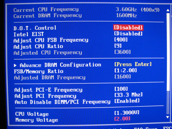
The MSI X48 Platinum allows for a certain degree of automatic overclocking. The D.O.T. (Dynamic Overclocking Technology) setting provides a means for setting the upper limit of this feature, either a 1, 3, or 5% increase in CPU frequency during periods of higher loading. Disabling this setting permits manual overclocking via Front Side Bus (FSB) and multiplier modifications. Half-multiplier support is included for Intel's newest 45nm processors.
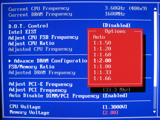
Available memory dividers are displayed in a slightly different manner than usual. These numbers correlate to 1:1, 6:5, 4:3, 3:2, 8:5, 5:3 and 2:1. Unfortunately, the only missing divider (5:4) is one of our favorites; hopefully MSI can work this into a future BIOS release.
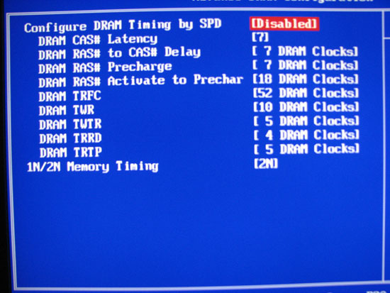
Selecting "Advanced DRAM Configuration" leads to a page where manual values can be entered, overriding the memory's SPD settings. Command Rate is also selectable at 1N or 2N - we have found that DDR3 is much more forgiving than DDR2 when it comes to selecting 1N at higher speeds. We would like to see a few more of the most common memory timings available for adjustment - tRC (Row Cycle Time) for example. MSI assures us that customer satisfaction is an important aspect of their business model, and they are constantly working to improve their products. We are also told that this BIOS is very early and we can expect some substantial enhancements in the next release.
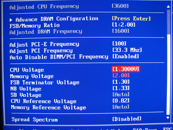
The X48 Platinum's use of a less traditional voltage monitor chip rendered CPU-Z incapable of reading actual CPU voltages in Windows. We did however check our processor's load voltages the old fashioned way, with a steady hand and a digital multimeter. Droop was not excessive and we found we could run just about the same VID settings with our QX9650 test processor as we could on any other board.
We were able to get away with leaving our "Memory Reference Voltage" on Auto (nominally one-half of memory voltage) but were forced to manually set the "CPU Reference Voltage" when working with our quad-core CPU. It appears as though the BIOS properly sets this voltage automatically when a dual-core CPU is installed, but it needs a little help with the QX9650. We used 0.82V with an "FSB Terminator Voltage" (VTT) of 1.30V - this being 63% of VTT. As you can see, the "CPU Reference Voltage" is really a single GTL setting in disguise. Without this change we were unable to press above about 360MHz FSB; afterwards we had no problems running 400MHz FSB.
As we mentioned before, higher "NB Voltage" settings has the effect of quickly causing instability. Switching to a more robust form of MCH cooling may help to alleviate this affect.
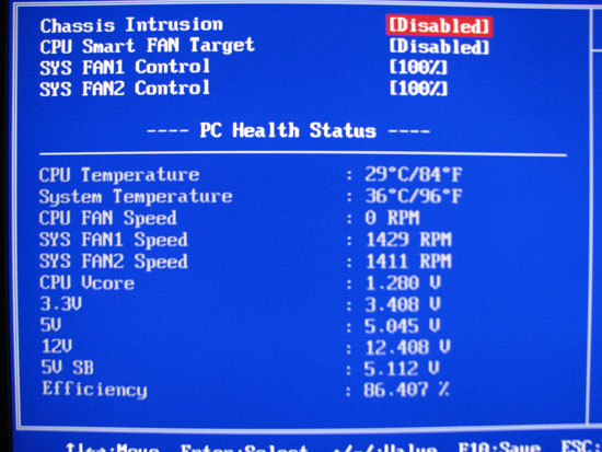
The in-BIOS hardware monitoring page is surprisingly good, although we would like to see NB voltage and memory voltage reported here. Those that do not have the ability to check these voltages on their own are usually comforted by the ability to easily verify these are where they think they should be. "System Temperature" is read out from somewhere near the PWM circuit and "CPU Temperature" is a reading from the processor's onboard temperature diode. Of these settings we were most intrigued by the one labeled "Efficiency". No doubt this refers to PWM efficiency but we have never seen this in a BIOS before.
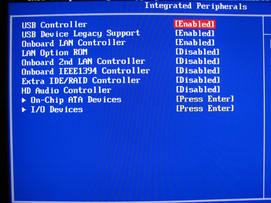
The last page we want to showcase contains options for enabling or alternately disabling some of the onboard controllers. "Extra IDE/RAID Controller" is a reference to the Marvell RAID controller with RAID 0/1 support; settings for the ICH9R are contained under "On-Chip ATA Devices".


21 Comments
View All Comments
HotBBQ - Thursday, January 31, 2008 - link
You cannot directly compare CAS latency across DDR revisions."Consider the latency ratings of the three most recent memory formats: Upper-midrange DDR-333 was rated at CAS 2; similar-market DDR2-667 was rated at CAS 4 and today's middle DDR3-1333 is often rated at CAS 8. Most people would be shocked to learn that these vastly different rated timings result in the same actual response time, which is specifically 12 nanoseconds." - Tomshardware
Mondoman - Friday, February 1, 2008 - link
Actually, you can compare the latency pretty directly across DDR technologies, as shown in your example. 2 clocks at DDR-333 = 4 (twice as fast) clocks at DDR2-667 = 8 (four times as fast) clocks at DDR3-1333.tayhimself - Thursday, January 31, 2008 - link
Please include stability testing. Who cares if you can get 1-5% more performance via exotic tweaks. Lets make sure that the board doesnt lock up when overclocked and laden with RAM by doing some stress testing. And make the stress testing transparent. These reviews are not as useful as or TR reviews for this reason.ATWindsor - Friday, February 1, 2008 - link
And also test if the product supports other things than graphic-cards in the PCIe-slots, a card like this begs for it.kjboughton - Thursday, January 31, 2008 - link
We will be including this type of information and much, much more in our upcoming X38/X48 motherboard round-up. As we mentioned in the review, this article is meant to provide you an early look at the layout, features, specifications, interesting BIOS options and a quick preview of any overclocking results. Stay tuned, we're confident we will address the concerns you brought to day in much more detail in just a short time.Vikendios - Thursday, January 31, 2008 - link
And please let us know how Nvidia cards work in SLI under Intel chipsets, not only under Nvidia's chipsets.I am particularly interested in twinned 8800 GT, since AnandTech called them "The only cards that matter".
OzoZoz - Thursday, January 31, 2008 - link
We all know that nVidia does not "certify" this Intel chipset to run SLI, but does that mean it won't work? I agree with Vikendios: I would like to see how SLI performs on these Intel-based motherboards.JarredWalton - Thursday, January 31, 2008 - link
I know of someone at a hardware site that was threatened with a lawsuit if they showed SLI performance on a non-NVIDIA system. (I don't know if those threats are still being sent around, but it wouldn't surprise me.) At present, the only way to make SLI work on a non-NVIDIA chipset requires a hack.Hacked drivers, but the latest drivers use some sort of encryption I believe so cracking them breaks the DMCA. I don't even know if anyone can break the encryption, and the last hacked drivers I heard about are quite old, XP only GeForce 7xxx or earlier only, and probably won't work with many modern games.
The other approach that might work would be to hack your BIOS so that it identifies itself as an nForce chipset. I don't know exactly what would be required for the ID string, or if it would work properly afterwards.
Note that SLI works on stuff like SkullTrail and PM945 (i.e. http://www.anandtech.com/mobile/showdoc.aspx?i=307...">in my Alienware m9750 review) because there's an nForce 100 bridge chip in use. nForce 100 is the precursor to the nForce 200 that's used to provide 780i with dual PCI-E 2.0 slots.
SoBizarre - Thursday, January 31, 2008 - link
It seems that the author of this article is very much “into” memory stuff. I have a little suggestion. Why don't you consider writing kind of “Everything about motherboards & RAM” guide. You could cover some practical aspects which are NEVER addressed by reviewers. For example: On motherboard supporting up to 8GB of RAM (like the one reviewed today), what is the limiting factor for RAM amount? Is it electrical(?) design of PCB, or is the address space limitation of chipset (BIOS)? Because if the BIOS can not address more than 8GB of memory, memory remapping will not help and you just can't have 8GB of RAM available to your (64bit) OS. Is that the case? Personally I don't run Virtual Machines nor do I have other reasons for installing 8GB of RAM , but other people do. Besides, it would be nice to just KNOW.smeister - Friday, February 1, 2008 - link
What's with the memory reference voltage?On the specification page (pg 2)
Memory Reference Voltage Auto, 0.90V ~ 1.25V
It should be half the DDR3 memory voltage
1.5V x 0.5 = 0.75V, so should be: Auto, 0.75V ~ 1.25V