AMD Tech Day at CES: 2018 Roadmap Revealed, with Ryzen APUs, Zen+ on 12nm, Vega on 7nm
by Ian Cutress on February 1, 2018 8:45 AM EST2nd Generation Ryzen
AMD has always stated that its Zen core design will form the basis of its high-performance x86 processors for the foreseeable future. This has included, among other things, a cadence with releasing updates and new Zen-like processor designs into the market. As announced at Tech Day, the update to 1st Generation Ryzen will be 2nd Generation Ryzen, coming in April 2018.
Specific core counts, frequencies, or model numbers were not mentioned – we are still 2-3 months away from this launch. AMD did state a number of points worth discussing however, especially with its decision to use GlobalFoundries newest 12nm ‘LP’ design process (12LP), compared to the 14nm ‘LPP’ design process (14LPP) used in the first generation Ryzen products.
First I want to go to this graph, to show what AMD want to claim on raw performance over the next three years:
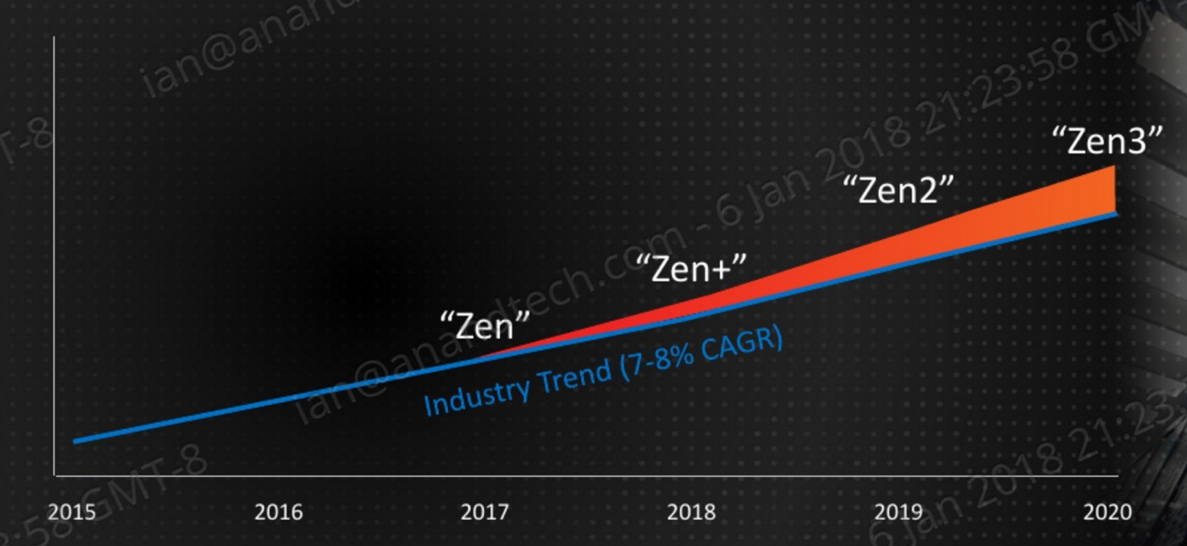
This is a graph of raw performance, combining both the efficiency of processing instructions (IPC, instructions per clock) as well as benefits from an improved manufacturing process. AMD cites the industry trend as growing 7-8% every year, and that they fully expect the Zen package, due to design improvements in the microarchitecture and better foundry notes, will go above and beyond that 7-8% figure.
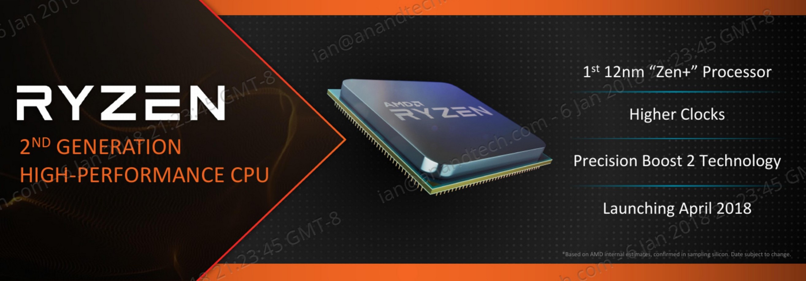
So first up along that line is Zen+. This will be the name of the core in the 2nd Generation Ryzen family, built on GlobalFoundries 12LP process. AMD has categorically stated that the core microarchitecture underneath has not changed: we will still have the same front-end and back-end as Zen, with the same size caches and the same layout. What has changed will be some of the power management algorithms, and perhaps some tweaks to the neural network-based prefetch algorithms. This will be headlined as ‘Precision Boost 2’ support, which is a feature that has already been introduced to the Ryzen with Vega graphics components (desktop and mobile).
GlobalFoundries 12LP
Most of the physical changes happen due to the process. Last year, AMD cited that its second generation Ryzen products will be on a ‘14+’ manufacturing node, but now it is going to be on a 12LP process. Some people argue that this is a clever marketing ploy as a name change, given nothing in the designs actually comes close to 14nm or 12nm. We were told that 12LP implements stricter design rules for the manufacturing process, requiring changes to library layout and the floorplan, but with an end result of a focus on performance per watt.
For the new processors, AMD is claiming a 10% boost in performance per watt overall. This is going to be taken as higher clocks for the same power at the high-end and lower power for the same frequency for more power sensitive products. AMD’s slide from Jim Anderson’s presentation above specifically says ‘higher clocks’, which when combined with Mark Papermaster’s presentation which states ‘10%+ performance vs. 14LPP’, we could take this to mean that we should expect anywhere from an 8%+ increase in frequencies with 2nd Generation Ryzen for desktop (not 10%, accounting for the fact that the power/efficiency curve gets worse the faster you are).
| Comparison of 14 nm Branded Process Technologies | |||||||
| GlobalFoundries 12LP |
GlobalFoundries 14HP |
GlobalFoundries 14LPP ? |
TSMC 16FF |
Intel 14nm |
|||
| Fin Pitch | ? | ? | ? | ? | 42 nm | ||
| Gate Pitch | ? | ? | 78 nm | 90 nm | 70 nm | ||
| Min Metal Pitch | ? | ? | 64 nm | 64 nm | 52 nm | ||
| Gate Height | ? | ? | less than 480 nm | 480 nm | 399 nm | ||
| Metal Layers | 13 | 17 | 13 | unknown | unknown | ||
| Design Library | 7.5T | 12T | 9T | 9T | unknown | ||
The 10% figure is corroborated by GlobalFoundries, who back in 2017 stated that its 12LP process will offer a 10% better performance. GF also stated that the 12LP process also offers a 15% area reduction against 14LPP. This is done, according to GlobalFoundries, by using 7.5T libraries rather than 9T libraries. This requires its customers to ‘recompile’ their 14LPP designs for the adjusted 12LP process.
To put this into context, this means we might see 4.3-4.5 GHz processors with the 2nd Generation Ryzen sticker where we used to see 4.0 GHz processors. It will be interesting to see how AMD and GlobalFoundries have moved that seemingly hard overclock limit we saw on processors like the Ryzen 7 1800X, which had a hard time moving past 4.2 GHz on all cores.
We are having a tour around GlobalFoundries Fab 8 in New York this week, and are set to spend some time with CTO Gary Patton, talking about the new process. While he is unlikely to quote specifically about how AMD has used the new design rules to its advantage, he might tell us some more information about the process in general.
As for 2nd Generation Ryzen, we are told that the major motherboard vendors and OEMs already have near-final engineering samples to hand to ensure updated compatibility.
New Motherboards: X470 Chipset and AM4 Motherboards
Launching around the same time as the new processors will be a range of X470 motherboards from the main motherboard manufacturers. Strictly speaking, these motherboards are not needed: the current AM4 motherboards based on the X370/B350/A320 chipsets on the market will accept the new processors (as well as APUs) with a relevant BIOS update. However, AMD plans to optimize its high-end chipset with a few new features.
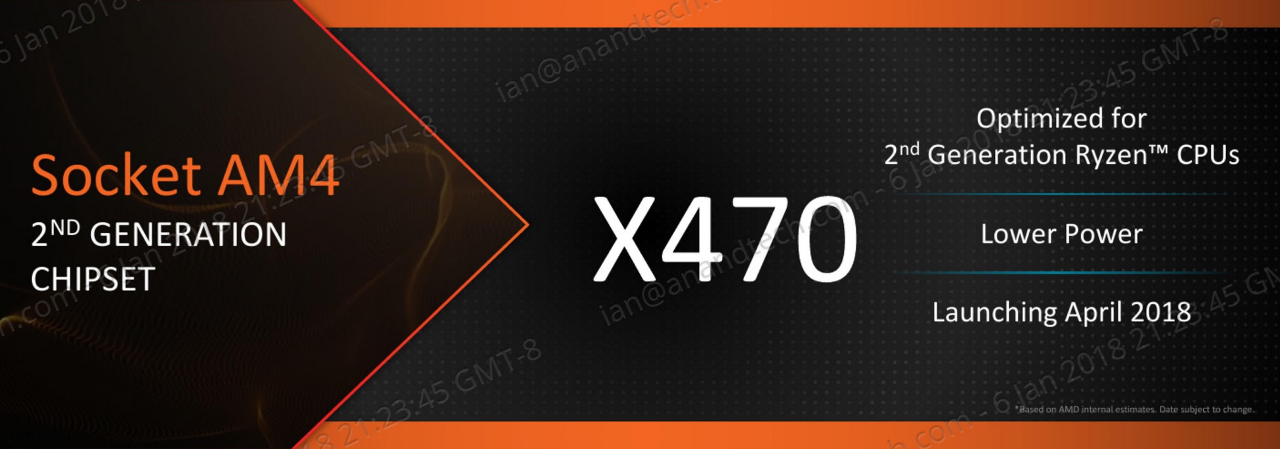
What we know so far is that the new X470 chipset is designed for lower power. How that is achieved, AMD would not go into at this point, however the fact that the X370 chipset was an outsourced product through ASMedia built on TSMC’s 55nm process would point to at least one way AMD could save power: building it on TSMC’s 40nm process for a start. We are told that the X370 and X470 chipsets are pin-compatible, which is not a limit to this theory, but an interesting point nonetheless.
AMD has stated that the new chipsets will be optimized better for the newer processors, which can be translated as better memory support and a few newer features. We were told that X470 will have very specific new features, although AMD did not want to disclose anything until we get closer to the launch.
We were lucky enough to see a GIGABYTE based X470 motherboard at CES.
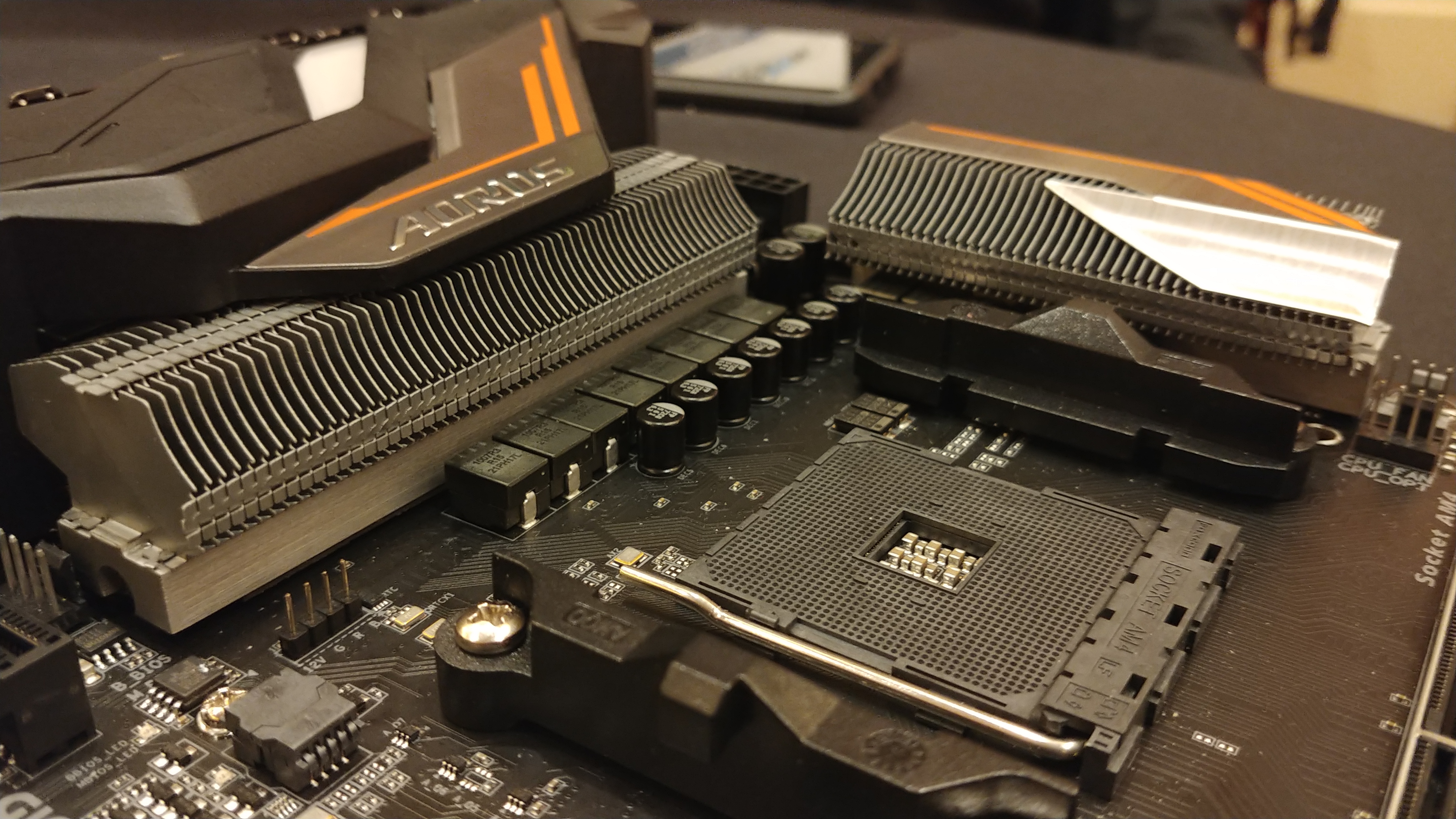
You can read our analysis on this motherboard here.
Second Generation Threadripper
In the second half of 2018, AMD will launch a second generation of Threadripper, based on the new 12LP process. AMD did not go into specific details here, mainly because the launch is so far away, but users should look forward to the same improvements as the standard Ryzen products: up to 10% better raw performance due to the improved manufacturing process, Precision Boost 2 support, and better memory compatibility.
We are not expecting anything to change on core counts or other features like PCIe lanes.


131 Comments
View All Comments
A5 - Monday, January 8, 2018 - link
Anything that is forbes.com/sites/* is not credible. You can literally go sign up for one right now if you want.And Forbes proper isn't credible on anything outside the financial industry.
iwod - Monday, January 8, 2018 - link
I mean Christ, you have financial industry reporter reporting on tech they barely understand and having reader that credit a non technical Journal pieces as creditable source and then attacking a journalist on a technical information site labelling him or her and the site as not creditable and when the journalist has a bloody Oxford PhD in the ElecChem Field.LurkingSince97 - Thursday, January 18, 2018 - link
LOL.GloFo announced LONG AGO that they were skipping the 10nm node and going straight from 14nm to 7nm. They mentioned that there would be some 14nm tweaks.
Other competitors started tweaking their 14nm / 16nm nodes and in some cases re-branded them (tsmc, IIRC rebranded a 16nm improvement as 12nm).
There is more than one feature size measurement in a process, being able to shrink a small subset of these by a little bit will allow for some increased density. Add on some other tweaks and you can lower power too. What do you call a heavily tweaked node that only shrinks a few of the feature sizes but not all? What number is half way between 14 and 10?
It doesn't really matter what they call it. Its ~ 10% faster or 10% lower power, with ~10% to 15% higher density.
The 12nm process is essentially a 14nm+, or ++. Its not a wholly new node. Fact 1: it will be incrementally deployed as a revision to the 14nm process where you start over nearly from scratch and almost the entire manufacturing pipeline is new. Fact 2: Unlike most minor tweaks, it does increase density. There is some justification in giving it a new size due to fact 2, but it is not a brand new process due to fact 1.
A truly new node takes _years_ to develop, not months. This appeared on their roadmap suddenly. Everyone and their brother (other than you) knew that they had a 14nm+ in the works -- AMD's roadmaps had "Zen+" on a GloFo "14nm+" node. Suddenly there was no more "14nm+" on AMD's roadmaps, and it was replaced with "12nm".
Significant tweaks to an existing node however,
LurkingSince97 - Thursday, January 18, 2018 - link
Ugh, I should proof-read:Fact 1: it will be incrementally deployed as a revision to the 14nm process where you start over nearly from scratch and almost the entire manufacturing pipeline is new.
Should say:
Fact 1: it will be incrementally deployed as an upgrade to the 14nm process (many of the manufacturing steps remain identical), while an entirely new node typically implies replacing almost the entire manufacturing pipeline.
Sane Indian - Monday, January 8, 2018 - link
"Acer will use the pre-announced higher-end APUs, the Ryzen 7 2700U and Ryzen 5 2500U, but will also be pairing this with a Radeon RX 560 graphics chip."Does iGPU and dGPU can crossfire or they just independently (switch from iGPU to dGPU and vice versa) depending upon power situation.
Ian Cutress - Monday, January 8, 2018 - link
Literally the rest of the paragraph answers the question.We were told by AMD that the integrated graphics and discrete graphics will be used in a switching context: for video playback, the lower power integrated graphics is used and the discrete is disabled, however the discrete graphics is fired up for gaming work. For compute, or for games that support multi-adaptor DirectX 12 technologies, both the integrated graphics and the discrete graphics should be available, however this is up to the game/software to implement.
Kevin G - Monday, January 8, 2018 - link
AMD executing right now and while there is argument that they've played it safe with Zen so far, they are in a very favorable position in the market. -"While most of the roadmap could have been predicted by those of us embedded in this industry, it was good to see AMD volunteering a lot of information. This can be a bit of a double-edged sword, if a competitor knows what you have planned". AMD knows that Intel's roadmap is in chaos as right now and pushing existing Zen designs to lower power envelopes and/or increasing clock speeds will close the performance gap. If Zen 2 advances in terms of IPC by any significant margin, they could actually pull ahead in 2019 but that entirely depends on Intel's response, in particular Ice Lake.Intel's missteps with 10 nm has left them open as the first Cannon Lake parts were due in late 2016! Meltdown and Spectre meltdown could have been the death blow to Cannon Lake as the incoming lawsuits make it unwise to release products with such significant flaws. Intel's server line up is also in chaos due to Meltdown/Spectre as Cascade Lake was pinned in as a stop-gap 14 nm solution before Cannon Lake-SP in 2019. Cascade lake for release this year should already be sampling but Meltdown/Spectre could force a delay. In particular is that Cascade Lake is supposed to support Optane DIMMs. The 10 nm Knight's Hill HPC processor has been cancelled roughly a month ago and replaced by Knight's Mill as a stop-gap for partners looking into AI. We'll probably find out later today when Intel's CEO takes the stage at CES.
wumpus - Monday, January 8, 2018 - link
"Death blow"? You seem to vastly overestimate the amount of silicon GoFlo can produce. Even if everything goes right for AMD, Intel will be shipping Cannon Lake chips left and right to consumers (the chips in the article appeared mostly for consumers) as GoFlo furiously produces Zepplin (or whatever its followup is called) and AMD ships them as hyperprofitable EPYC chips.That said, Intel certainly takes AMD competition seriously enough to throw together competing products such as the X299, even if such products make the rest of Intel look like they have no idea what they are doing. But still, massive gains for AMD will look like a tiny blip in Intel's revenue.
Orenj - Monday, January 8, 2018 - link
With Zen 2 already complete, I'm wondering if it contains any hardware assists for mitigation of Spectre-type attacks a la Intel's proposed IBRS/STIBP/IBPB?PixyMisa - Monday, January 8, 2018 - link
Unlikely; they've only known about this for a couple of months.