Analyzing Falkor’s Microarchitecture: A Deep Dive into Qualcomm’s Centriq 2400 for Windows Server and Linux
by Ian Cutress on August 20, 2017 11:00 AM EST- Posted in
- CPUs
- Qualcomm
- Enterprise
- SoCs
- Enterprise CPUs
- ARMv8
- Centriq
- Centriq 2400
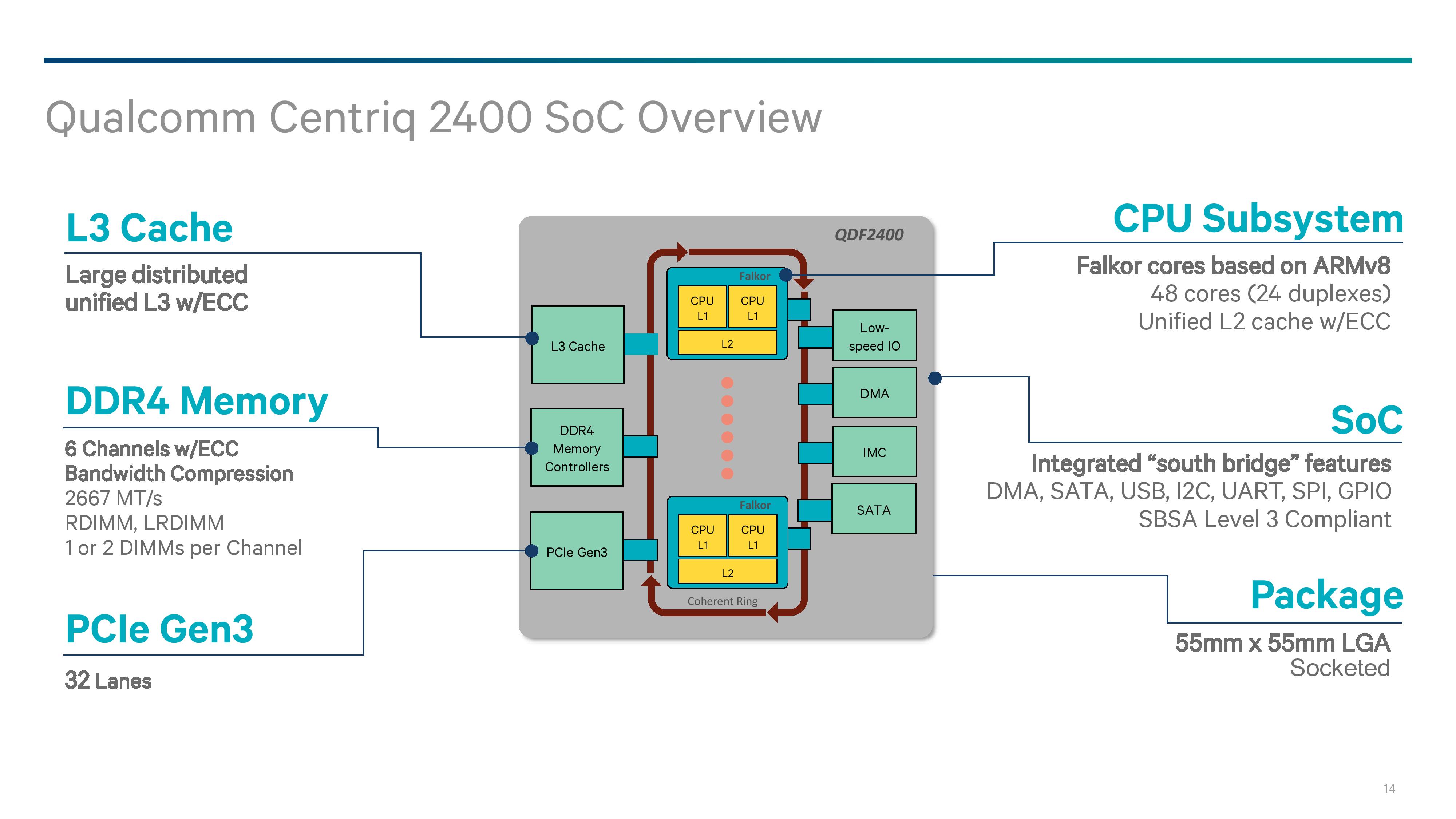
The SoC: 48 Falcor Cores, DDR4, PCIe
Two decades ago, when processors were a single core with external memory controllers, external caches, and external IO, routing was comparatively easier than what we have today. Now we have many core systems, multiple cache levels of different varieties, more IO than we can shake a stick at, and it all has to communicate with each other in a low power, low latency and high bandwidth way using a variety of interfaces. For the Centriq 2400, Qualcomm is implementing a number of enterprise requirements as well as integrating its own developed fabric.
For those that have been following our Intel/AMD coverage of late, we discussed how internal coherent fabrics are changing: Intel has moved from a ring-bus topology to a per-core networking mesh, and AMD uses its scalable Infinity Fabric within a die, between dies, between sockets, and from GPUs to memory. In the mobile space, coherent fabrics like ARMs CCI/CCN are typically all the rage, and ARM allows its partners to modify and tune those IPs as they need to (and most do). Rather than using off-the-shelf IP, Qualcomm has stated that its new interconnect is homegrown.
The Qualcomm System Bus (QSB) is a proprietary protocol based, bidirectional segmented ring bus. While Qualcomm shows a ring bus in the image above, we are told that the segmented ring bus might not exactly look like a ring inside the chip – by creating a segmented core-to-core design, it means the cores might not be in a ring at all, with some elements sprouting from off shoots and cores having more than one direction to travel. If Qualcomm were to share a false-color die shot, this would likely be visible. The QSB also allows for multicast on read as well as shortest path routing, which again sounds more like a mesh based networking implementation. Qualcomm quotes a >250GB/s aggregate bandwidth for the QSB.
On the Fabric is everything the system needs: cores, cache, memory, PCIe and IO.
The Centriq family will implement a pair of Falkor cores into a Falkor ‘Duplex’, where each core with have a private L1 cache and a shared L2 cache with ECC. We’ll cover the Falkor design in the next few pages.
For the L3 cache, Qualcomm has not quoted a size but has said that it will scale with the number of cores on the chip. In the above slide it states that it is a distributed unified cache, which can be confusing. Ultimately the cache is fully accessible from all cores, unless a QoS policy is in play, but the cache is likely segmented to allow for the relevant QoS policy tags to bind certain regions to certain cores/VMs. Despite it saying unified, it means that there will be partitions of the L3 around the QSB interconnect. The L3 will be with ECC as well.
Memory controllers are also accessed from the QSB interconnect, with the Centriq 2400 supporting six memory channels of up to DDR4-2667 at up to 2 DIMMs per channel. Support will include RDIMM and LRDIMM, which would suggest up to 1.5TB of LRDIMM support per socket using 128GB LRDIMMs, similar to Intel’s premium memory offerings.
Connectivity comes via 32 lanes of PCIe 3.0, which falls below that offered by Intel (32-44, fewer when chipset level Quick Assist or 10GbE is being used), AMD (128 PCIe in 1P or 2P), X-Gene 3 (42), or Cavium. We probed Qualcomm on features such as NVMe, NVMe RAID, and fall-over support, although in our limited time briefing there was not time to cover it – we might hear more while we are at Hot Chips this week.
Qualcomm has designed the chip as a true SoC such that it doesn’t need a chipset. We’ve confirmed that this is on-die connectivity, rather than via a multi-chip package add-in. The information we have states that the chip will support the usual array of SATA, USB, I2C, UART, GPIO and DMA, although how much of anything has not been stated.


41 Comments
View All Comments
SarahKerrigan - Sunday, August 20, 2017 - link
I seriously doubt SVE is present. As far as I know, Fujitsu is still lined up to be the first SVE user, and it's not like ultra-wide vectors are a massive boost to conventional enterprise servers.Kevin G - Sunday, August 20, 2017 - link
Using SVE requires ARM v8.2A support which this does not appear to have. The ARM v8.2A spec only was announced in January 2016, which isn't enough time to get it implemented into anything that'd be shipping now. Qualcomm could have been working behind the scenes but that would have given them perhaps another year with a spec that could change before formal publishing (i.e. may require some last minute changes right past the design would be tapping out). For a server part, that path would be unwise.SVE was announced a year ago and is far more complex than the v8.2A released due to how it handles execution width. A SVE design right now is a virtual impossibility.
Hurr Durr - Sunday, August 20, 2017 - link
I`d rather read something on x86 thing on ARM that MS and Qualcomm have than this. Much more potential for the real world.Kevin G - Sunday, August 20, 2017 - link
Can we get an editor in here?"For SoC design followers, one might look at this design and think they see similarities with designs such as AMD’s original Bulldozer design from 2011. ... Actually, after writing that last sentence, it is basically a Xeon Phi dual core module."
While perfectly readable, that last paragraph could use a bit of a rewrite due to the last sentence nullifying it. My quick stab at a rewrite:
For SoC followers, the Qualcomm pairs two modules per fabric stop similar to what Intel has implemented in their most recent Xeon Phi chips. Unlike the new grid topology in the Xeon Phi, Qualcomm is using a ring bus akin to what Intel uses on its Xeon E5 and E7 chips. Those thinking that a dual core module would follow AMD's Bulldozer philosophy will be disappointed to learn that no execution resources are shared between the cores, just the L2 cache, power management and bus interface.
The same comparisons and ideas are made but they flow to the reader a bit more logically to me.
FunBunny2 - Sunday, August 20, 2017 - link
-- Unlike the new grid topology in the Xeon Phi, Qualcomm is using a ring bus akin to what Intel uses on its Xeon E5 and E7 chips.I've long wondered how hardware engineers:
1) discover such alternatives
2) decide which one to choose
Is this fundamental math and physics laws, or trial and error? anyone know a readable (for the non-physics major, that is) source?
Kevin G - Monday, August 21, 2017 - link
Topology has been a well studied concept. At a high level, this mimics general networking design closely. The choice of on-die topology is generally at the mercy of engineering trade offs that are unique in this context.The ring bus you get an easy means of scaling the number of units but the trade of is an increase in latency around the ring bus as the numbers go up. Diminishing returns are hit as the numbers increases. With a ring though, individual units on the ring can be radically different sizes on a die as long the links between stops can be roughly the same for timing purposes. A ring bus also permits a relatively predictable latency to reach stops further away, something noteworthy for implementing coherency protocols. Another trade off with the ring design is that it'll always consume power. Nodes that are not in use still need to have the ring stop going to permit data passage through it.
Qualcomm side steps the ring issue a little bit by including two cores per ring stop, thus putting the minimum number of stops at 24. Just like Intel, I suspect on-die IO like PCIe, memory controllers etc. will have their own ring stops. It is not clear if this all on one massive ring bus or like the last generation of E5/E7 high core count chips, several rings are used with discrete bridges between them. Intel never went beyond 16 ring stops in a design.
A grid topology requires far greater engineering resources to implement correctly. Physical size has to be the same for those nodes in the middle of the grid but there is a bit of wiggle room along the perimeter to expand in one of the two dimensions (handy for things like PCIe, memory controllers that have a fixed need per socket). Cache coherency has to account for variable latency between nodes on the grid: there are several paths to between source and destination. The main benefit of a grid though is that scaling is vastly improved as core count increases. Another benefit is that not all the links in between cores needs to be active to move data. This saves power. Due to the ability to route around congested links, the individual links between grid nodes do not necessarily have to be as wide as those on a ring, saving a bit of energy there while maintaining similar aggregate bandwidth. For servers, multi-pathing of data (ie sending it twice) is also possible for increased RAS if an error in transmit is encountered along a particular path. Intel hasn't indicated that they're doing multipathing but could be a feature they add down the road. In the future if chips stacking emerges outside of research labs as feasible, the grid topology can also expand into the 3rd dimension.
The recent Xeon Phi isn't Intel's first attempt at a grid topology. The first publiclly shown off design was there Terascale research chip a decade ago. ( http://www.eetimes.com/document.asp?doc_id=1303295 ) Inter core topology was a major driver of that research effort and the recent Xeon Phi and Xeon series are the result of those efforts. Intel isn't event the first to implement a grid topology. The Compaq/DEC Alpha EV7 did so between sockets and permitted up to 64 sockets in an 8 x 8 grid from the early 2000's. IBM used a grid-like design for their BlueGene super computer designs to move data, though that wasn't cache coherent. There could be earlier instances as those are a few that I know off hand.
FunBunny2 - Monday, August 21, 2017 - link
thanks. much clearer.Ryan Smith - Sunday, August 20, 2017 - link
Thanks!Lord-Bryan - Sunday, August 20, 2017 - link
"So we have to admit that we were surprised by Qualcomm releasing so much information about the pipeline. When we’ve ever asked the mobile CPU team about Krait and Kryo, we usually hit a brick wall, left with a PR answer of a ‘custom core design’ or the guide of ‘protecting our design"Well am not surprised, releasing architectural details of server cpus, has always been an industry norm. It is something they just have to do if they want to be relevant, you can't just sell black boxes worth thousands of dollars to just anyone.
Lord-Bryan - Sunday, August 20, 2017 - link
Plus developers will have to know how the processor works in other to optimize applications for it, Qualcomm is playing with the big boys now, no room for unnecessary pride.