Sizing Up Servers: Intel's Skylake-SP Xeon versus AMD's EPYC 7000 - The Server CPU Battle of the Decade?
by Johan De Gelas & Ian Cutress on July 11, 2017 12:15 PM EST- Posted in
- CPUs
- AMD
- Intel
- Xeon
- Enterprise
- Skylake
- Zen
- Naples
- Skylake-SP
- EPYC
Memory Subsystem: Latency
The performance of modern CPUs depends heavily on the cache subsystem. And some applications depend heavily on the DRAM subsystem too. We used LMBench in an effort to try to measure cache and memory latency. The numbers we looked at were "Random load latency stride=16 Bytes".
| Mem Hierarchy |
AMD EPYC 7601 DDR4-2400 |
Intel Skylake-SP DDR4-2666 |
Intel Broadwell Xeon E5-2699v4 DDR4-2400 |
| L1 Cache cycles | 4 | 4 | 4 |
| L2 Cache cycles | 12 | 14-22 | 12-15 |
| L3 Cache 4-8 MB - cycles | 34-47 | 54-56 | 38-51 |
| 16-32 MB - ns | 89-95 ns | 25-27 ns (+/- 55 cycles?) |
27-42 ns (+/- 47 cycles) |
| Memory 384-512 MB - ns | 96-98 ns | 89-91 ns | 95 ns |
Previously, Ian has described the AMD Infinity Fabric that stitches the two CCXes together in one die and interconnects the 4 different "Zeppelin" dies in one MCM. The choice of using two CCXes in a single die is certainly not optimal for Naples. The local "inside the CCX" 8 MB L3-cache is accessed with very little latency. But once the core needs to access another L3-cache chunk – even on the same die – unloaded latency is pretty bad: it's only slightly better than the DRAM access latency. Accessing DRAM is on all modern CPUs a naturally high latency operation: signals have to travel from the memory controller over the memory bus, and the internal memory matrix of DDR4-2666 DRAM is only running at 333 MHz (hence the very high CAS latencies of DDR4). So it is surprising that accessing SRAM over an on-chip fabric requires so many cycles.
What does this mean to the end user? The 64 MB L3 on the spec sheet does not really exist. In fact even the 16 MB L3 on a single Zeppelin die consists of two 8 MB L3-caches. There is no cache that truly functions as single, unified L3-cache on the MCM; instead there are eight separate 8 MB L3-caches.
That will work out fine for applications that have a footprint that fits within a single 8 MB L3 slice, like virtual machines (JVM, Hypervisors based ones) and HPC/Big Data applications that work on separate chunks of data in parallel (for example, the "map" phase of "map/reduce"). However this kind of setup will definitely hurt the performance of applications that need "central" access to one big data pool, such as database applications and big data applications in the "Shuffle phase".
Memory Subsystem: TinyMemBench
To double check our latency measurements and get a deeper understanding of the respective architectures, we also use the open source TinyMemBench benchmark. The source was compiled for x86 with GCC 5.4 and the optimization level was set to "-O3". The measurement is described well by the manual of TinyMemBench:
Average time is measured for random memory accesses in the buffers of different sizes. The larger the buffer, the more significant the relative contributions of TLB, L1/L2 cache misses, and DRAM accesses become. All the numbers represent extra time, which needs to be added to L1 cache latency (4 cycles).
We tested with dual random read, as we wanted to see how the memory system coped with multiple read requests.
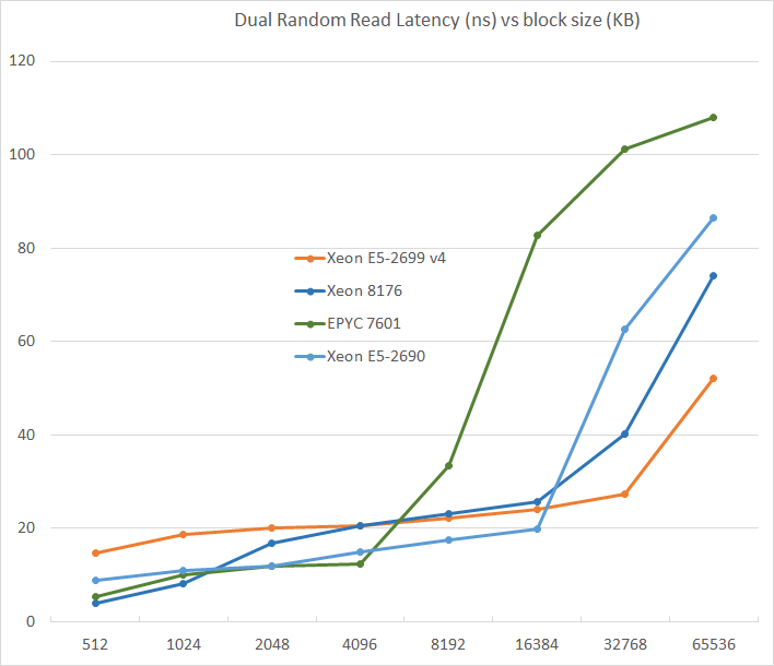
L3-cache sizes have increased steadily over the years. The Xeon E5 v1 had up to 20 MB, v3 came with 45 MB, and v4 "Broadwell EP" further increased this to 55 MB. But the fatter the cache, the higher the latency became. L3 latency doubled from Sandy Bridge-EP to Broadwell-EP. So it is no wonder that Skylake went for a larger L2-cache and a smaller but faster L3. The L2-cache offers 4 times lower latency at 512 KB.
AMD's unloaded latency is very competitive under 8 MB, and is a vast improvement over previous AMD server CPUs. Unfortunately, accessing more 8 MB incurs worse latency than a Broadwell core accessing DRAM. Due to the slow L3-cache access, AMD's DRAM access is also the slowest. The importance of unloaded DRAM latency should of course not be exaggerated: in most applications most of the loads are done in the caches. Still, it is bad news for applications with pointer chasing or other latency-sensitive operations.


219 Comments
View All Comments
Panxa - Sunday, July 16, 2017 - link
"Competition has spoiled the naming convention Intels 14 === competetions 7 or 10"The node naming convention used to be the gate length, however that has become irrelevant. Intel 14 nm gate lenghth is about 1.5x and 10 nm about 1.8x. Companies and organizations have developed quite accurate models to asses process density with equations based on process poarameters like CPP and MPP to what they call a "standard node"
"Intel used to maintain 2 year lead now grew that to 3-4year lead"
Don't belive intel propaganda. Intel takes the lead in 2014 with their 14nm process with a standard node value of 12.1. Samsung and then TSMC take the lead in 2017 with their 10nm processes having standard node values of 11.2 and 10.3 respectively. Intel will retake the the lead back when they deliver their 10nm process with a standard node value of 8.3. However it will be a short lived lead, TSMC will retake the lead back with their 7nm with a standard node of 7.9 before GLOBALFOUNDRIES takes the lead in 2018 with their 7nm process with a standard node value of 7.8. The gap is gone !!!
"yet their revenue profits grow year over year"
Wrong. Intel revenue for the last years remained fairly constant
2011 grow
2012 decline
2013 decline
2014 grow
2015 decline
2016 grow
All in all from 2011 to 2016 revenue went from 54 billion to 59 billion. If we take into account inflation $54 billion in the year 2011 is worth $58.70 billion today.
Not to mention that Samsung has overtaken Intel to become the world No.1 semiconductor company, and that a "pure play" foundry like TSMC has surpassed intel in market CAP
johnp_ - Wednesday, July 12, 2017 - link
The Xeon Bronze Table on Page 7 seems to have an error. It lists the 4112 as having 5.50MB L3, but ark says it has 8.25MB, just like the 3104, so it looks like it has an above-average L3/Core:https://ark.intel.com/products/123551
Ian Cutress - Friday, July 14, 2017 - link
I've got Intel documents from our briefings that say it has the regular 1.375MB/core allocation, and others saying it has 8.25MB. I'm double checking.johnp_ - Friday, July 21, 2017 - link
All commercial listings and most reviews I've seen online show the processor with 8.25MB as well.Do you have any further information from Intel?
pepoluan - Wednesday, July 12, 2017 - link
What I'm dying to know: Performance when running as virtualization host. Using Xen, VMware, and Hyper-V.Threska - Saturday, July 22, 2017 - link
Virtualization itself, and more importantly virtualization security.Sparkyman215 - Wednesday, July 12, 2017 - link
Typo here: Intel will seven different versions of the chipset, varying in 10G and QAT support, but also varying in TDP:tmbm50 - Wednesday, July 12, 2017 - link
One thing to consider when considering value is the Microsoft Server 2016 core tax.....assuming your mission critical apps are still tied to MS ;-)Server 2016 now chargers per core with an 8 core socket as the base. The Window license for a 32 core server is NUTS.
I'm surprised AMD and Intel are not pushing Microsoft on this. For datacenters like ourselves its pushing us to 8 core sku's with more 2U nodes.
msroadkill612 - Wednesday, July 12, 2017 - link
Aye, its a fuuny world lad.The way the automobile panned out differently in different countries, was laargely die to fuel tax regimes, rather than technology.
i.e. what is the best way to cheat a bit on the incumbent tax rules of germany/france/uk vs a more laissez faire USA. In UK, u were taxed on horsepower, but u could cheat a bit w/ hi revs & more gears - that sort of thing.
rahvin - Wednesday, July 12, 2017 - link
Who runs any Windows service on bare metal these days? If you haven't virtulalized your windows servers running on KVM you should.