Sizing Up Servers: Intel's Skylake-SP Xeon versus AMD's EPYC 7000 - The Server CPU Battle of the Decade?
by Johan De Gelas & Ian Cutress on July 11, 2017 12:15 PM EST- Posted in
- CPUs
- AMD
- Intel
- Xeon
- Enterprise
- Skylake
- Zen
- Naples
- Skylake-SP
- EPYC
Memory Subsystem: Latency
The performance of modern CPUs depends heavily on the cache subsystem. And some applications depend heavily on the DRAM subsystem too. We used LMBench in an effort to try to measure cache and memory latency. The numbers we looked at were "Random load latency stride=16 Bytes".
| Mem Hierarchy |
AMD EPYC 7601 DDR4-2400 |
Intel Skylake-SP DDR4-2666 |
Intel Broadwell Xeon E5-2699v4 DDR4-2400 |
| L1 Cache cycles | 4 | 4 | 4 |
| L2 Cache cycles | 12 | 14-22 | 12-15 |
| L3 Cache 4-8 MB - cycles | 34-47 | 54-56 | 38-51 |
| 16-32 MB - ns | 89-95 ns | 25-27 ns (+/- 55 cycles?) |
27-42 ns (+/- 47 cycles) |
| Memory 384-512 MB - ns | 96-98 ns | 89-91 ns | 95 ns |
Previously, Ian has described the AMD Infinity Fabric that stitches the two CCXes together in one die and interconnects the 4 different "Zeppelin" dies in one MCM. The choice of using two CCXes in a single die is certainly not optimal for Naples. The local "inside the CCX" 8 MB L3-cache is accessed with very little latency. But once the core needs to access another L3-cache chunk – even on the same die – unloaded latency is pretty bad: it's only slightly better than the DRAM access latency. Accessing DRAM is on all modern CPUs a naturally high latency operation: signals have to travel from the memory controller over the memory bus, and the internal memory matrix of DDR4-2666 DRAM is only running at 333 MHz (hence the very high CAS latencies of DDR4). So it is surprising that accessing SRAM over an on-chip fabric requires so many cycles.
What does this mean to the end user? The 64 MB L3 on the spec sheet does not really exist. In fact even the 16 MB L3 on a single Zeppelin die consists of two 8 MB L3-caches. There is no cache that truly functions as single, unified L3-cache on the MCM; instead there are eight separate 8 MB L3-caches.
That will work out fine for applications that have a footprint that fits within a single 8 MB L3 slice, like virtual machines (JVM, Hypervisors based ones) and HPC/Big Data applications that work on separate chunks of data in parallel (for example, the "map" phase of "map/reduce"). However this kind of setup will definitely hurt the performance of applications that need "central" access to one big data pool, such as database applications and big data applications in the "Shuffle phase".
Memory Subsystem: TinyMemBench
To double check our latency measurements and get a deeper understanding of the respective architectures, we also use the open source TinyMemBench benchmark. The source was compiled for x86 with GCC 5.4 and the optimization level was set to "-O3". The measurement is described well by the manual of TinyMemBench:
Average time is measured for random memory accesses in the buffers of different sizes. The larger the buffer, the more significant the relative contributions of TLB, L1/L2 cache misses, and DRAM accesses become. All the numbers represent extra time, which needs to be added to L1 cache latency (4 cycles).
We tested with dual random read, as we wanted to see how the memory system coped with multiple read requests.
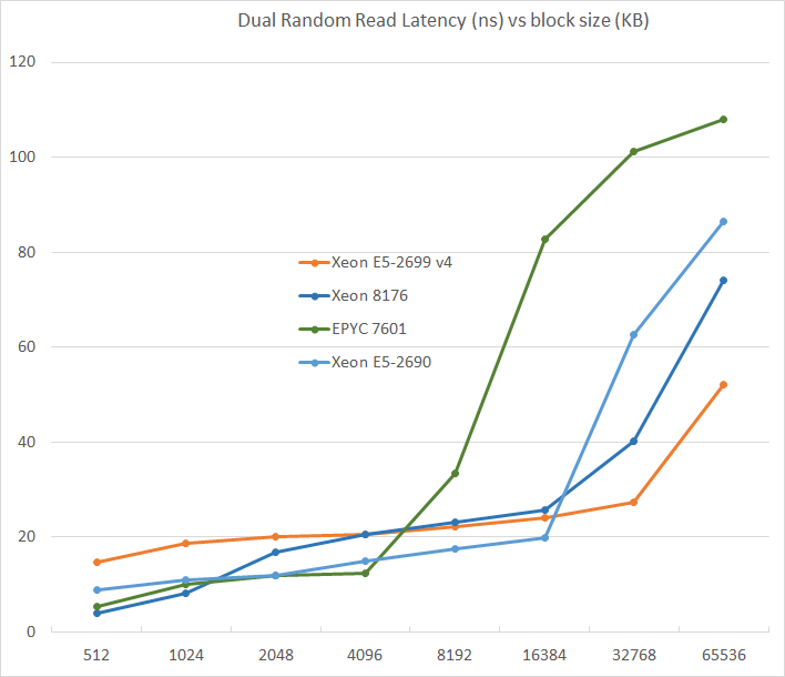
L3-cache sizes have increased steadily over the years. The Xeon E5 v1 had up to 20 MB, v3 came with 45 MB, and v4 "Broadwell EP" further increased this to 55 MB. But the fatter the cache, the higher the latency became. L3 latency doubled from Sandy Bridge-EP to Broadwell-EP. So it is no wonder that Skylake went for a larger L2-cache and a smaller but faster L3. The L2-cache offers 4 times lower latency at 512 KB.
AMD's unloaded latency is very competitive under 8 MB, and is a vast improvement over previous AMD server CPUs. Unfortunately, accessing more 8 MB incurs worse latency than a Broadwell core accessing DRAM. Due to the slow L3-cache access, AMD's DRAM access is also the slowest. The importance of unloaded DRAM latency should of course not be exaggerated: in most applications most of the loads are done in the caches. Still, it is bad news for applications with pointer chasing or other latency-sensitive operations.


219 Comments
View All Comments
PixyMisa - Tuesday, July 11, 2017 - link
No, the pricing is correct. The 1P CPUs really are half the price of a single 2P CPU.msroadkill612 - Wednesday, July 12, 2017 - link
Seems to me, the simplest explanation of something complex, is to list what it will not do, which they will not do :(.Can i run a 1p Epyc in a 2p mobo e.g., please?
PixyMisa - Thursday, July 13, 2017 - link
Short answer is no. It might boot, but only half the slots, memory, SATA and so on will be available. Two 1P CPUs won't talk to each other.A 2P Epyc will work in a 1P board though.
cekim - Tuesday, July 11, 2017 - link
One glaring bug/feature of AMD's segmentation relative to Intel's is the utter and obvious crippling of clock speeds for all but the absolute top SKUs. Fewer cores should be able to make use of higher clocks within the same TDP envelope. As a result Intel is objectively offering more and better fits up and down the sweep of cores vs clocks vs price spectrum.So, the bottom line is AMD is saying that you will have to buy the top-end, 4S SKU to get the top GHz for those applications in your mix that won't benefit from 16,18,32,128 cores.
I say all of this as someone who desperately wants EPYC to shake things up and force Intel to remove the sand-bags. I know I'm in a small, but non-zero market of users who can make use of dozens of cores, but still need 8 or fewer cores to perform on par with desktop parts for that purpose.
KAlmquist - Wednesday, July 12, 2017 - link
One possibility is that they have only a small percentage of the chips currently being produced bin well enough to be used in the highest clocking SKU's, so they are saving those chips for the most expensive offerings. Admittedly, that depends on what they are seeing coming off the production line. If they have a fair number of chips where with two very good cores, and two not so good, then it would make sense to offer a high clocking 16 core EPYC using chips with two cores disabled. But if clock speed on most chips is limited due to minor registration errors (which would affect the entire chip), then a chip with only two really good cores would require two localized defects in two separate cores, in addition to very good registration to get the two good cores. The combination might be too rare to justify a separate SKU.I would expect Global Foundries to continue to tweak its process to get better yields. In that case, more processors would end up in the highest bin, and AMD might decide to launch a higher clock speed 16 and 8 core EPYC processors, mostly using chips which bin well enough that they could have been used for the 32 core EPYC 7601.
alpha754293 - Tuesday, July 11, 2017 - link
Why does the Intel Xeon 6142 cost LESS than the 6142M? (e.g. per the table above, 6142 is shown with a price of $5946 while the 6142M costs $2949)ca197 - Tuesday, July 11, 2017 - link
I assume that is the wrong way round on the list. I have seen it reported the other way round on other sites.Ian Cutress - Tuesday, July 11, 2017 - link
You're correct. I've updated the piece, was a misread error from Intel's tables.coder543 - Tuesday, July 11, 2017 - link
On page 6, it says that Epyc only has 64 PCIe lanes (available), but that's not correct. There are 128 PCIe lanes per chip. In a 1P configuration, that's 128 PCIe lanes available. On a 2P configuration, 64 PCIe lanes from each chip are used to connect to the other chip, leaving 64 + 64 = 128 PCIe lanes still available.This is a significant advantage.
Ian Cutress - Tuesday, July 11, 2017 - link
You misread that table. It's quoting per-CPU when in a 2P configuration.