Intel Announces Skylake-X: Bringing 18-Core HCC Silicon to Consumers for $1999
by Ian Cutress on May 30, 2017 3:03 AM ESTAnnouncement Three: Skylake-X's New L3 Cache Architecture
(AKA I Like Big Cache and I Cannot Lie)
SKU madness aside, there's more to this launch than just the number of cores at what price. Deviating somewhat from their usual pattern, Intel has made some interesting changes to several elements of Skylake-X that are worth discussing. Next is how Intel is implementing the per-core cache.
In previous generations of HEDT processors (as well as the Xeon processors), Intel implemented an three stage cache before hitting main memory. The L1 and L2 caches were private to each core and inclusive, while the L3 cache was a last-level cache covering all cores and that also being inclusive. This, at a high level, means that any data in L2 is duplicated in L3, such that if a cache line is evicted into L2 it will still be present in the L3 if it is needed, rather than requiring a trip all the way out to DRAM. The sizes of the memory are important as well: with an inclusive L2 to L3 the L3 cache is usually several multiplies of the L2 in order to store all the L2 data plus some more for an L3. Intel typically had 256 kilobytes of L2 cache per core, and anywhere between 1.5MB to 3.75MB of L3 per core, which gave both caches plenty of room and performance. It is worth noting at this point that L2 cache is closer to the logic of the core, and space is at a premium.
With Skylake-X, this cache arrangement changes. When Skylake-S was originally launched, we noted that the L2 cache had a lower associativity as it allowed for more modularity, and this is that principle in action. Skylake-X processors will have their private L2 cache increased from 256 KB to 1 MB, a four-fold increase. This comes at the expense of the L3 cache, which is reduced from ~2.5MB/core to 1.375MB/core.
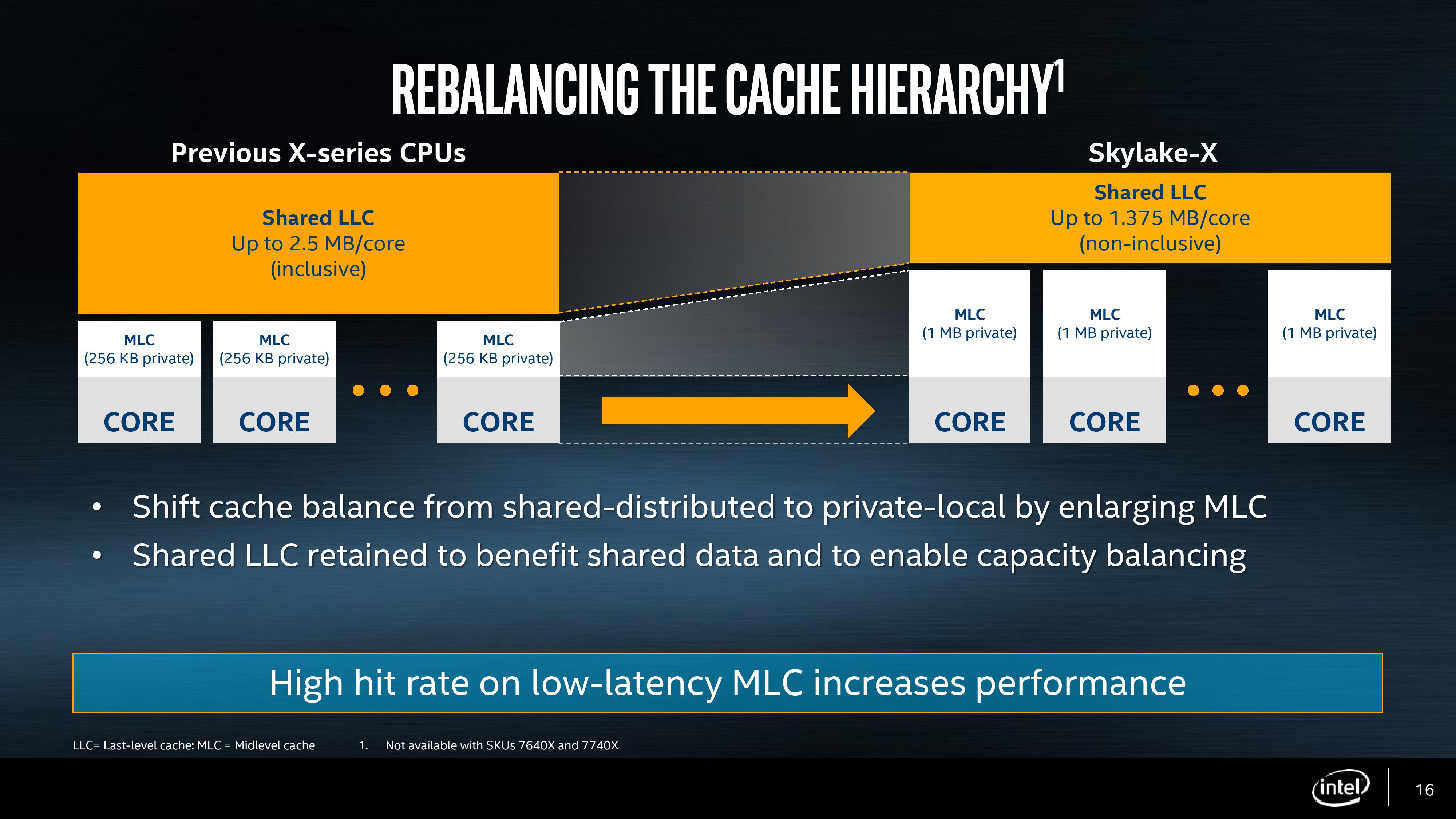
With such a large L2 cache, the L2 to L3 connection is no longer inclusive and now ‘non-inclusive’. Intel is using this terminology rather than ‘exclusive’ or ‘fully-exclusive’, as the L3 will still have some of the L3 features that aren’t present in a victim cache, such as prefetching. What this will mean however is more work for snooping, and keeping track of where cache lines are. Cores will snoop other cores’ L2 to find updated data with the DRAM as a backup (which may be out of date). In previous generations the L3 cache was always a backup, but now this changes.
The good element of this design is that a larger L2 will increase the hit-rate and decrease the miss-rate. Depending on the level of associativity (which has not been disclosed yet, at least not in the basic slide decks), a general rule I have heard is that a double of cache size decreases the miss rate by the sqrt(2), and is liable for a 3-5% IPC uplift in a regular workflow. Thus here’s a conundrum for you: if the L2 has a factor 2 better hit rate, leading to an 8-13% IPC increase, it’s not the same performance as Skylake-S. It may be the same microarchitecture outside the caches, but we get a situation where performance will differ.
Fundamental Realisation: Skylake-S IPC and Skylake-X IPC will be different.
This is something that fundamentally requires in-depth testing. Combine this with the change in the L3 cache, and it is hard to predict the outcome without being a silicon design expert. I am not one of those, but it's something I want to look into as we approach the actual Skylake-X launch.
More things to note on the cache structure. There are many ‘ways’ to do it, one of which I imagined initially is a partitioned cache strategy. The cache layout could be the same as previous generations, but partitions of the L3 were designated L2. This makes life difficult, because then you have a partition of the L2 at the same latency of the L3, and that brings a lot of headaches if the L2 latency has a wide variation. This method would be easy for silicon layout, but hard to implement. Looking at the HCC silicon representation in our slide-deck, it’s clear that there is no fundamental L3 covering all the cores – each core has its partition. That being the case, we now have an L2 at approximately the same size as the L3, at least per core. Given these two points, I fully suspect that Intel is running a physical L2 at 1MB, which will give the design the high hit-rate and consistent low-latency it needs. This will be one feather in the cap for Intel.


203 Comments
View All Comments
Gothmoth - Sunday, June 4, 2017 - link
so true (linus about x299):https://www.youtube.com/watch?v=TWFzWRoVNnE
it´s intel doing as less as possible to make as much money as possible....
and customers are stupid enough to defend that.
yes it capitalism.. but i would be stupid as a customer to like it.
AMD is offering me more at the moment so i decide with my wallet.
Timoo - Saturday, June 10, 2017 - link
A little late, but I think it is worth mentioning:Linus' review of the i9.
Scrapped to pieces...https://www.youtube.com/watch?v=TWFzWRoVNnE
Gothmoth - Monday, June 12, 2017 - link
64 PCI lanes for under 900 euro or 44 pci lanes for over 900 euro... mhm let me think about it.....