The AMD Zen and Ryzen 7 Review: A Deep Dive on 1800X, 1700X and 1700
by Ian Cutress on March 2, 2017 9:00 AM ESTZen: New Core Features
Since August, AMD has been slowly releasing microarchitecture details about Zen. Initially it started with a formal disclosure during Intel’s annual developer event, the followed a paper at HotChips, some more details at the ‘New Horizon’ event in December, and recently a talk at ISSCC. The Zen Tech Day just before launch gave a chance to get some of those questions answered.
First up, let’s dive right in to the high-level block diagram:
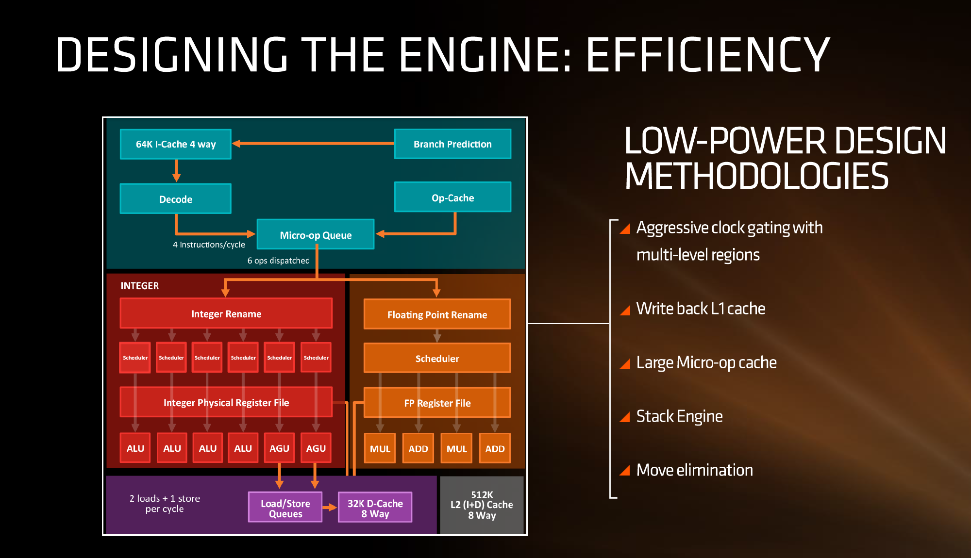
In this diagram, the core is split into the ‘front-end’ in blue and the rest of the core is the ‘back-end’. The front-end is where instructions come into the core, branch predictors are activated and instructions are decoded into micro-ops (micro-operations) before being placed into a micro-op queue. In red is the part of the back-end that deals with integer (INT) based instructions, such as integer math, loops, loads and stores. In orange is the floating-point (FP) part of the back-end, typically focused on different forms of math compute. Both the INT and FP segments have their own separate execution port schedulers
If it looks somewhat similar to other high-performance CPU cores, you’d be correct: there seems to be a high-level way of ‘doing things’ when it comes to x86, with three levels of cache, multi-level TLBs, instruction coalescing, a set of decoders that dispatch a combined 4-5+ micro-ops per cycle, a very large micro-op queue (150+), shared retire resources, AVX support, and simultaneous hyper-threading.
What’s New to AMD
First up, and the most important, was the inclusion of the micro-op cache. This allows for instructions that were recently used to be called up to the micro-op queue rather than being decoded again, and saves a trip through the core and caches. Typically micro-op caches are still relatively small: Intel’s version can support 1536 uOps with 8-way associativity. We learned (after much asking) at AMD’s Tech Day that the micro-op cache for Zen can support ‘2K’ (aka 2048) micro-ops with up to 8-ops per cache line. This is good for AMD, although I conversed with Mike Clark on this: if AMD had said ‘512’, on one hand I’d be asking why it is so small, and on the other wondering if they would have done something different to account for the performance adjustments. But ‘2K’ fits in with what we would expect.
Secondly is the cache structure. We were given details for the L1, L2 and L3 cache sizes, along with associativity, to compare it to former microarchitectures as well as Intel’s offering.
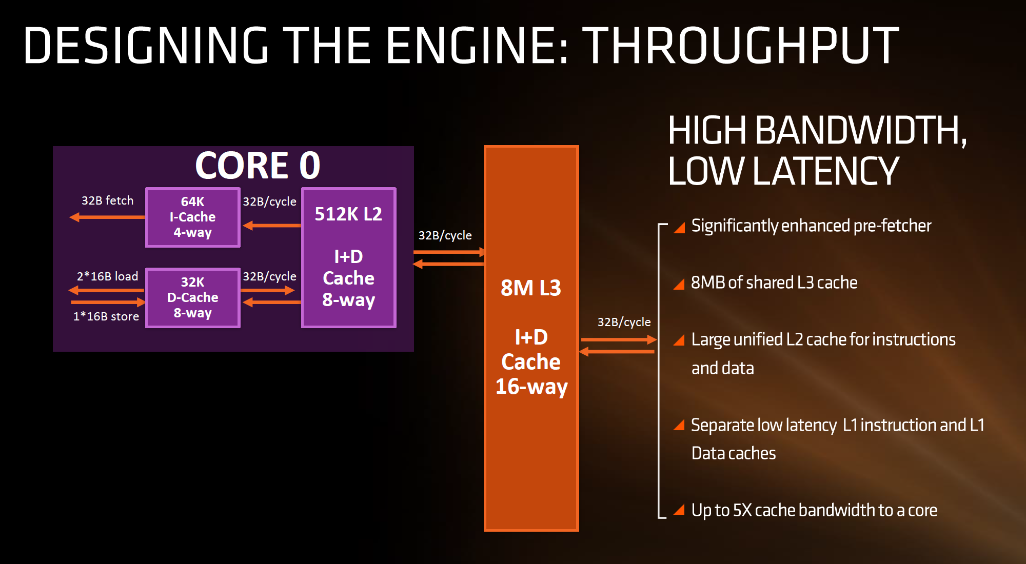
In this case, AMD has given Zen a 64KB L1 Instruction cache per core with 4-way associativity, with a lop-sided 32KB L1 Data cache per core with 8-way associativity. The size and accessibility determines how frequently a cache line is missed, and it is typically a trade-off for die area and power (larger caches require more die area, more associativity usually costs power). The instruction cache, per cycle, can afford a 32byte fetch while the data cache allows for 2x 16-byte loads and one 16-byte store per cycle. AMD stated that allowing two D-cache loads per cycle is more representative of the most workloads that end up with more loads than stores.
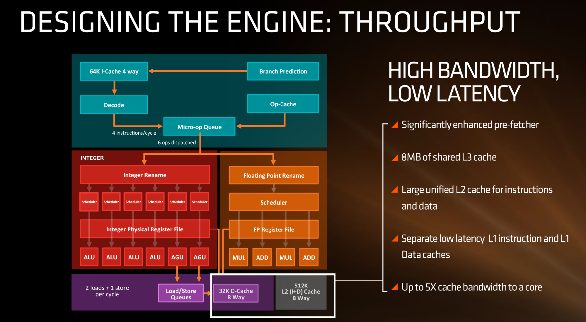
The L2 is a large 512 KB, 8-way cache per core. This is double the size of Intel’s 256 KB 4-way cache in Skylake or 256 KB 8-way cache in Broadwell. Typically doubling the cache size affords a 1.414 (square root of 2) better chance of a cache hit, reducing the need to go further out to find data, but comes at the expense of die area. This will have a big impact on a lot of performance metrics, and AMD is promoting faster cache-to-cache transfers than previous generations. Both the L1 and L2 caches are write-back caches, improving over the L1 write-through cache in Bulldozer.
The L3 cache is an 8MB 16-way cache, although at the time last week it was not specified over how many cores this was. From the data release today, we can confirm rumors that this 8 MB cache is split over a four-core module, affording 2 MB of L3 cache per core or 16 MB of L3 cache for the whole 8-core Zen CPU. These two 8 MB caches are separate, so act as a last-level cache per 4-core module with the appropriate hooks into the other L3 to determine if data is needed. As part of the talk today we also learned that the L3 is a pure victim cache for L1/L2 victims, rather than a cache for prefetch/demand data, which tempers the expectations a little but the large L2 will make up for this. We’ll discuss it as part of today’s announcement.
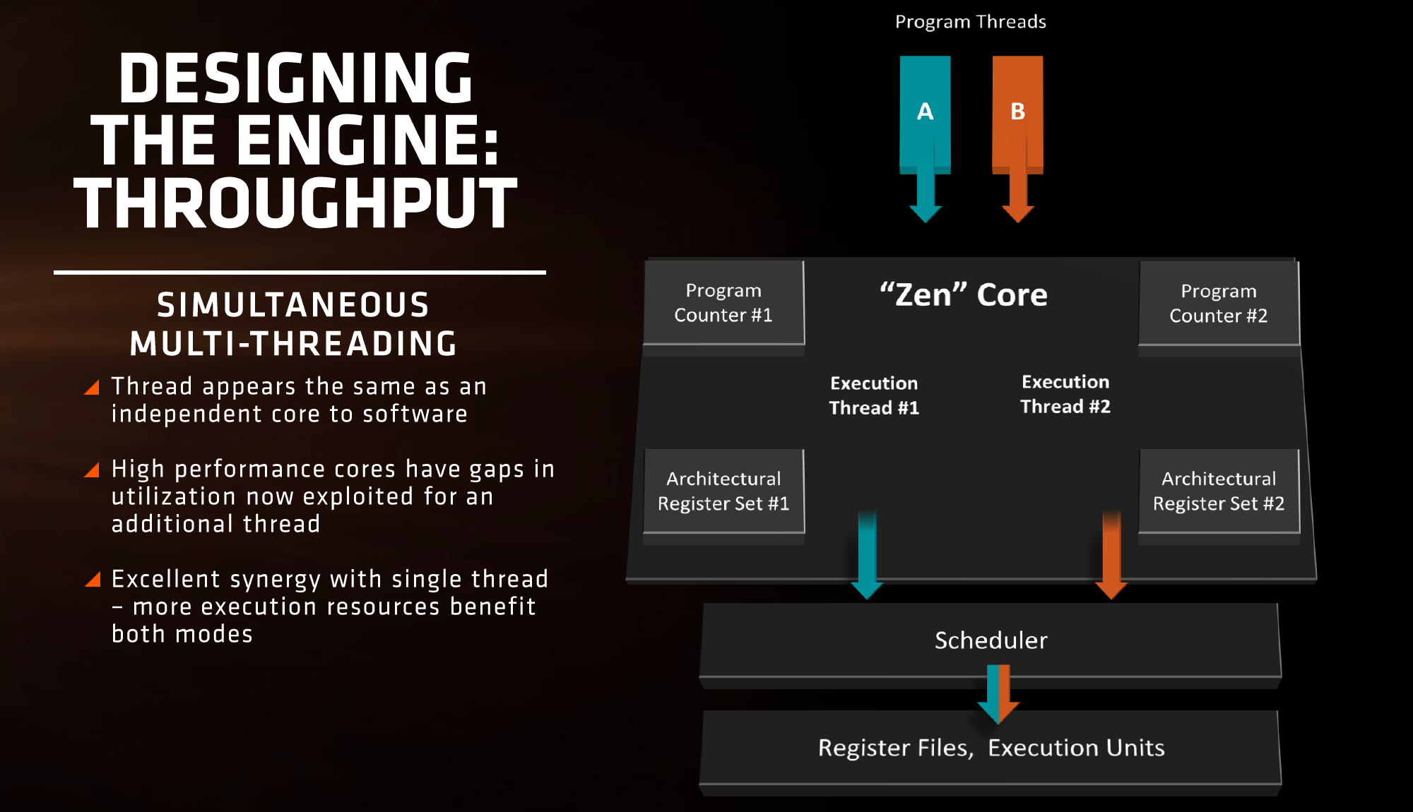
AMD is also playing with SMT, or simultaneous multi-threading. We’ve covered this with Intel extensively, under the heading ‘HyperThreading’. At a high level both these terms are essentially saying the same thing, although their implementations may differ. Adding SMT to a core design has the potential to increase throughput by allowing a second thread (or third, or fourth, or like IBM up to eight) on the same core to have the same access to execution ports, queues and caches. However SMT requires hardware level support – not all structures can be dynamically shared between threads and can either be algorithmically partitioned (prefetch), statically partitioned (micro-op queue) or used in alternate cycles (retire queue).
We also have dual schedulers, one for INT and another for FP, which is different to Intel’s joint scheduler/buffer implementation.


574 Comments
View All Comments
nt300 - Saturday, March 11, 2017 - link
If AMD hadn't gone with GF's 14nm process, ZEN would probably have been delayed. I think as soon as Ryzen Optimizations come out, these chips will further outperform.MongGrel - Thursday, March 9, 2017 - link
For some reason making a casual comment about anything bad about the chip will get you banned at the drop of a hat on the tech forums, and then if you call him out they will ban you more.
https://arstechnica.com/gadgets/2017/03/amds-momen...
MongGrel - Thursday, March 9, 2017 - link
For some reason, MarkFW seems to thinks he is the reincarnation of Kyle Bennet, and whines a lot before retreating to his safe space.nt300 - Saturday, March 11, 2017 - link
I've noticed in the past that AMD has an issue with increasing L3 cache speed and/or Latencies. Hopefully they start tightening the L3 as much as possible. Can Anandtech do a comparison between Ryzen before Optimizations and after Optimizations. Tyalpha754293 - Friday, March 17, 2017 - link
Looks like that for a lot of the compute-intensive benchmarks, the new Ryzen isn't that much better than say a Core i5-7700K.That's quite a bit disappointing.
AMD needs to up their FLOPS/cycle game in order to be able to compete in that space.
Such a pity because the original Opterons were a great value proposition vs. the Intels. Now, it doesn't even come close.
deltaFx2 - Saturday, March 25, 2017 - link
@Ian Cutress: When you do test gaming, if you can, I'd love to have the hypothesis behind the 'generally accepted methodology' tested out. The methodology being, to test it at lowest resolution. The hypothesis is that this stresses the CPU, and that a future, higher performance GPU will be bottlenecked by the slower CPU. Sounds logical, but is it?Here's the thing: Typically, when given more computing resources, people scale up their problem to utilize those resources. In other words, if I give you a more powerful GPU, games will scale up their perf requirements to match it, by doing stuff that were not possible/practical in earlier GPUs. Today's games are far more 'realistic' and are played at much higher resolutions than say 5 years ago. In which case, the GPU is always the limiting factor no matter what (unless one insists on playing 5 year old games on the biggest, baddest GPU). And I fully expect that the games of today are built to max out current GPUs, so hardware lags software.
This has parallels with what happens in HPC: when you get more compute nodes for HPC problems, people scale up the complexity of their simulations rather than running the old, simplified simulations. Amdahl's law is still not a limiting factor for HPC, and we seem to be talking about Exascale machines now. Clearly, there's life in HPC beyond what a myopic view through the Amdahl law lens would indicate.
Just a thought :) Clearly, core count requirements have gone up over the last decade, but is it true that a 4c/8t sandy bridge paired up with Nvidia's latest and greatest is CPU-bottlenecked at likely resolutions?
wavelength - Friday, March 31, 2017 - link
I would love to see Anand test against AdoredTV's most recent findings on Ryzen https://www.youtube.com/watch?v=0tfTZjugDegLawJikal - Friday, April 21, 2017 - link
What I'm surprised to see missing... in virtually all reviews across the web... is any discussion (by a publication or its readers) on the AM4 platform's longevity and upgradability (in addition to its cost, which is readily discussed).Any Intel Platform - is almost guaranteed to not accommodate a new or significantly revised microarchitecture... beyond the mere "tick". In order to enjoy a "tock", one MUST purchase a new motherboard (if historical precedent is maintained).
AMD AM4 Platform - is almost guaranteed to, AT LEAST, accommodate Ryzen "II" and quite possibly Ryzen "III" processors. And, in such cases, only a new processor and BIOS update will be necessary to do so.
This is not an insignificant point of differentiation.
PeterCordes - Monday, June 5, 2017 - link
The uArch comparison table has some errors for the Intel columns. Dispatch/cycle: Skylake can read 6 uops per clock from the uop cache into the issue queue, but the issue stage itself is still only 4 uops wide. You've labelled Even running from the loop buffer (LSD), it can only sustain a throughput of 4 uops per clock, same 4-wide pipeline width it has been since Core2. (pre-Haswell it has to be a mix of ALU and some store or load to sustain that throughput without bottlenecking on the execution ports.) Skylake's improved decode and uop-cache bandwidth lets it refill the uop queue (IDQ) after bubbles in earlier stages, keeping the issue stage fed (since the back-end is often able to actually keep up).Ryzen is 6-wide, but I think I've read that it can only issue 6 uops per clock if some of them are from "double instructions". e.g. 256-bit AVX like VADDPS ymm0, ymm1, ymm2 that decodes to two separate 128-bit uops. Running code with only single-uop instructions, the Ryzen's front-end throughput is 5 uops per clock.
In Intel terminology, "dispatch" is when the scheduler (aka Reservation Station) sends uops to the execution units. The row you've labelled "dispatch / cycle" is clearly the throughput for issuing uops from the front-end into the out-of-order core, though. (Putting them into the ROB and Reservation Station). Some computer-architecture people call that "dispatch", but it's probably not a good idea in an x86 context. (Unless AMD uses that terminology; I'm mostly familiar with Intel).
----
You list the uop queue size at 128 for Skylake. This is bogus. It's always 64 per thread, with or without hyperthreading. Intel has alternated in SnB/IvB/HSW/SKL between this and letting one thread use both queues as a single big queue. HSW/BDW statically partition their 56-entry queue into two 28-entry halves when two threads are active, otherwise it's a 56-entry queue. (Not 64). Agner Fog's microarch pdf and Intel's optmization manual both confirm this (in Section 2.1.1 about Skylake's front-end improvements over previous generations).
Also, the 4-uop per clock issue width is 4 fused-domain uops, so I was able to construct a loop that runs 7 unfused-domain uops per clock (http://www.agner.org/optimize/blog/read.php?i=415#... with 2 micro-fused ALU+load, one micro-fused store, and a dec/branch. AMD doesn't talk about "unfused" uops because it doesn't use a unified scheduler, IIRC, so memory source operands always stay with the ALU uop.
Also, you mentioned it in the text, but the L1d change from write-through to write-back is worth a table row. IIRC, Bulldozer's L1d write-back has a small buffer or something to absorb repeated writes of the same lines, so it's not quite as bad as a classic write-through cache would be for L2 speed/power requirements, but Ryzen is still a big improvement.