The AMD Zen and Ryzen 7 Review: A Deep Dive on 1800X, 1700X and 1700
by Ian Cutress on March 2, 2017 9:00 AM ESTZen: New Core Features
Since August, AMD has been slowly releasing microarchitecture details about Zen. Initially it started with a formal disclosure during Intel’s annual developer event, the followed a paper at HotChips, some more details at the ‘New Horizon’ event in December, and recently a talk at ISSCC. The Zen Tech Day just before launch gave a chance to get some of those questions answered.
First up, let’s dive right in to the high-level block diagram:
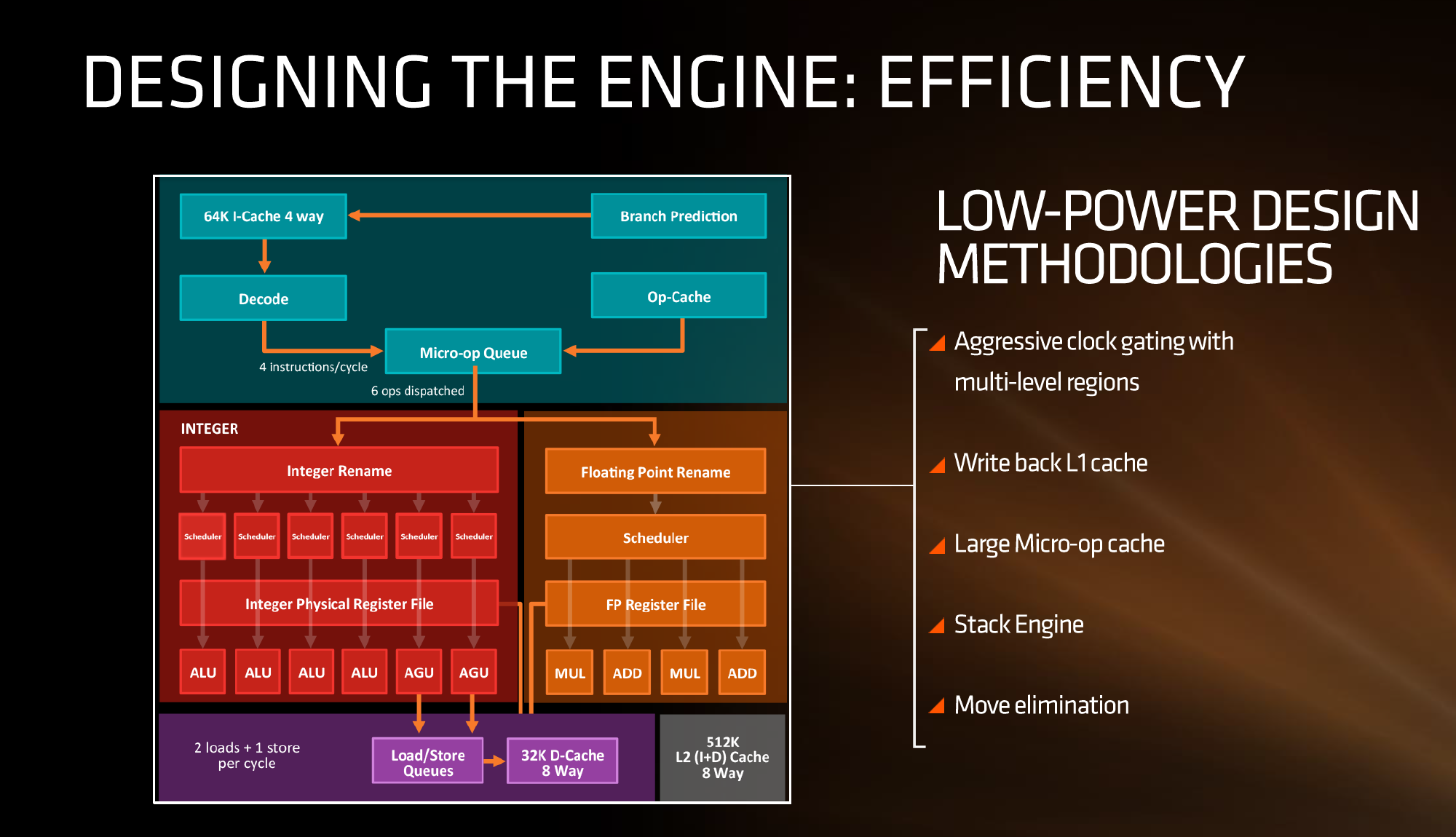
In this diagram, the core is split into the ‘front-end’ in blue and the rest of the core is the ‘back-end’. The front-end is where instructions come into the core, branch predictors are activated and instructions are decoded into micro-ops (micro-operations) before being placed into a micro-op queue. In red is the part of the back-end that deals with integer (INT) based instructions, such as integer math, loops, loads and stores. In orange is the floating-point (FP) part of the back-end, typically focused on different forms of math compute. Both the INT and FP segments have their own separate execution port schedulers
If it looks somewhat similar to other high-performance CPU cores, you’d be correct: there seems to be a high-level way of ‘doing things’ when it comes to x86, with three levels of cache, multi-level TLBs, instruction coalescing, a set of decoders that dispatch a combined 4-5+ micro-ops per cycle, a very large micro-op queue (150+), shared retire resources, AVX support, and simultaneous hyper-threading.
What’s New to AMD
First up, and the most important, was the inclusion of the micro-op cache. This allows for instructions that were recently used to be called up to the micro-op queue rather than being decoded again, and saves a trip through the core and caches. Typically micro-op caches are still relatively small: Intel’s version can support 1536 uOps with 8-way associativity. We learned (after much asking) at AMD’s Tech Day that the micro-op cache for Zen can support ‘2K’ (aka 2048) micro-ops with up to 8-ops per cache line. This is good for AMD, although I conversed with Mike Clark on this: if AMD had said ‘512’, on one hand I’d be asking why it is so small, and on the other wondering if they would have done something different to account for the performance adjustments. But ‘2K’ fits in with what we would expect.
Secondly is the cache structure. We were given details for the L1, L2 and L3 cache sizes, along with associativity, to compare it to former microarchitectures as well as Intel’s offering.
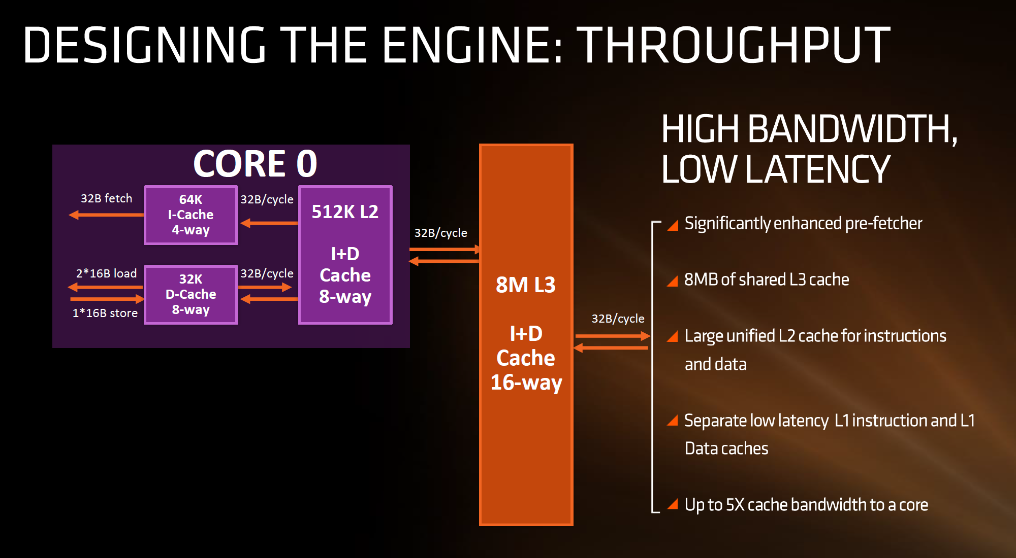
In this case, AMD has given Zen a 64KB L1 Instruction cache per core with 4-way associativity, with a lop-sided 32KB L1 Data cache per core with 8-way associativity. The size and accessibility determines how frequently a cache line is missed, and it is typically a trade-off for die area and power (larger caches require more die area, more associativity usually costs power). The instruction cache, per cycle, can afford a 32byte fetch while the data cache allows for 2x 16-byte loads and one 16-byte store per cycle. AMD stated that allowing two D-cache loads per cycle is more representative of the most workloads that end up with more loads than stores.
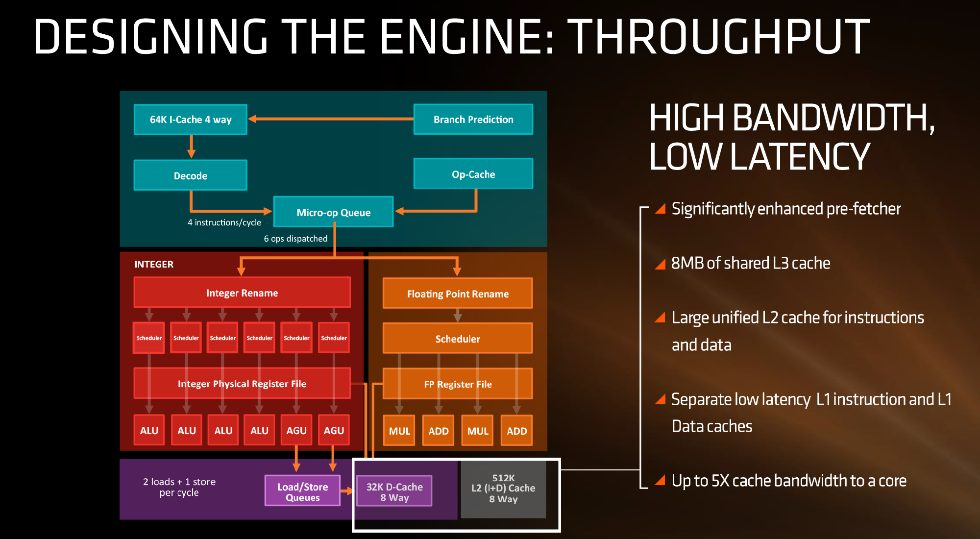
The L2 is a large 512 KB, 8-way cache per core. This is double the size of Intel’s 256 KB 4-way cache in Skylake or 256 KB 8-way cache in Broadwell. Typically doubling the cache size affords a 1.414 (square root of 2) better chance of a cache hit, reducing the need to go further out to find data, but comes at the expense of die area. This will have a big impact on a lot of performance metrics, and AMD is promoting faster cache-to-cache transfers than previous generations. Both the L1 and L2 caches are write-back caches, improving over the L1 write-through cache in Bulldozer.
The L3 cache is an 8MB 16-way cache, although at the time last week it was not specified over how many cores this was. From the data release today, we can confirm rumors that this 8 MB cache is split over a four-core module, affording 2 MB of L3 cache per core or 16 MB of L3 cache for the whole 8-core Zen CPU. These two 8 MB caches are separate, so act as a last-level cache per 4-core module with the appropriate hooks into the other L3 to determine if data is needed. As part of the talk today we also learned that the L3 is a pure victim cache for L1/L2 victims, rather than a cache for prefetch/demand data, which tempers the expectations a little but the large L2 will make up for this. We’ll discuss it as part of today’s announcement.
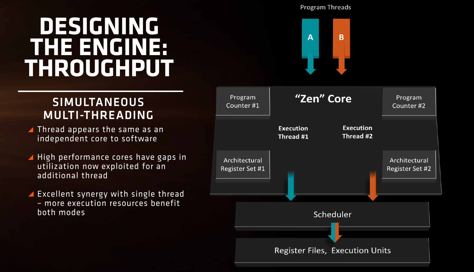
AMD is also playing with SMT, or simultaneous multi-threading. We’ve covered this with Intel extensively, under the heading ‘HyperThreading’. At a high level both these terms are essentially saying the same thing, although their implementations may differ. Adding SMT to a core design has the potential to increase throughput by allowing a second thread (or third, or fourth, or like IBM up to eight) on the same core to have the same access to execution ports, queues and caches. However SMT requires hardware level support – not all structures can be dynamically shared between threads and can either be algorithmically partitioned (prefetch), statically partitioned (micro-op queue) or used in alternate cycles (retire queue).
We also have dual schedulers, one for INT and another for FP, which is different to Intel’s joint scheduler/buffer implementation.


574 Comments
View All Comments
Cooe - Sunday, February 28, 2021 - link
Find me these so-called people buying Intel HEDT CPU's (aka OG Ryzen 7's direct competition) for gaming & never for HPC uses.... Oh wait. They don't exist.Haawser - Thursday, March 2, 2017 - link
Yeah, but if you're a gamer who streams, Ryzen is waaaay better than anything Inter offer for $499. Especially if you're gaming at 4K, or going to be. Different people have different needs, even gamers.Jimster480 - Thursday, March 2, 2017 - link
Yes but no,Because Broadwell-E and Haswell-E HEDT platforms are in the same boat as Ryzen.
But this is what this Ryzen 7 release is meant to do.
Compete with the HEDT platforms, not against the "APU" chips.
Those chips will come later, albeit with much higher clockspeeds to compete with intel.
For now you have Intel with 10-20% clockspeed advantages in clockspeed dependent applications.
Meteor2 - Saturday, March 4, 2017 - link
I hope you're right but there's no indication they will be clocked higher. AMD has access to processes which are generation behind Intel's, at least for a couple of years. We can't expect miracles.nos024 - Thursday, March 2, 2017 - link
Lol, butt hurt? Why even bother running gaming benchmarks? You even said it yourself that ryzen wont make it to your so called grown-up workstation because if low pcie count.So tell me who is this $500 Ryzen chip designed for? Not grown ups running workstation, or pathetic kiddies gamers...so theyre for Wannabes?
Tunnah - Thursday, March 2, 2017 - link
He literally said it is ideal to replace his aging 3770k, he gave an example of how it will be used. Try more reading and less being a turdddriver - Thursday, March 2, 2017 - link
Ryzen is that much more affordable that with the price difference I could have built another whole system, dedicated to running the 2 HBA adapters, thus saving on the need of 16 lanes. 40 - 16 is exactly 24, which is what ryzen has. If it was available a year ago I would have simply built two systems, offering a good 50-60% more CPU performance, double the GPU performance, with enough need to accommodate my IO needs, even if between two systems, that wouldn't have been much of an issue.The pci lane count is lower than intel E series chips, however it is still 50% higher than what you can get from intel outside the E series. It will actually suffice in most workstation scenarios, even if you end up running graphics at x8, which is not really a big deal.
ddriver - Thursday, March 2, 2017 - link
"you even said it yourself that ryzen wont make it to your so called grown-up workstation because if low pcie count"I did not say that. Not all workstations require 40 pcie lanes. Most could do with 24. I was talking about my workstation in particular, which has plenty of pcie hardware. For the vast majority of HPC scenarios that would not be necessary, furthermore as already mentioned, with the saved money you can build additional systems dedicated to specific tasks, offloading both the need of more pcie lanes and the cpu time the attached hardware consumes.
It remains to be seen how much IO will the server zen parts have. Ryzen is not particularly a workstation grade chip, it just happens to be GOOD ENOUGH to do the job. AMD give you 50% more performance and 50% more IO at the same or better price point, and I think they will do the same for the chips they actually design for workstation.
It looks like the 16 core workstation chip will have 64 pcie lanes, and the 32 core - a whooping 128 lanes. So intel E series looks like a sad little orphan with its modest 40 lanes... And no, xeons aren't much better, they are in fact worse, the 24 core E7-8894 v4 only has a modest 32 lanes.
So no, while I will not be replacing my main 10 core workstation with a ryzen, because that would win me nothing, I am definitely looking forward to replacing it next year with a Naples system, and I definitely wished ryzen was available last year as I could have spent my money much better than buying intel.
Intel999 - Thursday, March 2, 2017 - link
"So tell me who is this $500 Ryzen chip designed for?"Logic would imply it is aimed at anyone that works in an environment where they need superior multithreading performance. For instance, anyone that has bought a 6900k or 6950k, but more importantly it is for those individuals that "wanted" to buy either of Intel's multi core champs but couldn't due to ridiculous prices.
I'd dare to make a bet there are more people that wanted to buy a 6900k than there are people that actually did. Now they can buy one and still put food on the table this month.
FriendlyUser - Thursday, March 2, 2017 - link
Exactly right. I was always tempted by the 6850K, but the price of the CPU+platform was simply ridiculous. For much less I got a faster CPU and a high-end MB. I won't miss the 40PCIe lanes.