Hidden Secrets: Investigation Shows That NVIDIA GPUs Implement Tile Based Rasterization for Greater Efficiency
by Ryan Smith on August 1, 2016 5:00 AM EST
As someone who analyzes GPUs for a living, one of the more vexing things in my life has been NVIDIA’s Maxwell architecture. The company’s 28nm refresh offered a huge performance-per-watt increase for only a modest die size increase, essentially allowing NVIDIA to offer a full generation’s performance improvement without a corresponding manufacturing improvement. We’ve had architectural updates on the same node before, but never anything quite like Maxwell.
The vexing aspect to me has been that while NVIDIA shared some details about how they improved Maxwell’s efficiency over Kepler, they have never disclosed all of the major improvements under the hood. We know, for example, that Maxwell implemented a significantly altered SM structure that was easier to reach peak utilization on, and thanks to its partitioning wasted much less power on interconnects. We also know that NVIDIA significantly increased the L2 cache size and did a number of low-level (transistor level) optimizations to the design. But NVIDIA has also held back information – the technical advantages that are their secret sauce – so I’ve never had a complete picture of how Maxwell compares to Kepler.
For a while now, a number of people have suspected that one of the ingredients of that secret sauce was that NVIDIA had applied some mobile power efficiency technologies to Maxwell. It was, after all, their original mobile-first GPU architecture, and now we have some data to back that up. Friend of AnandTech and all around tech guru David Kanter of Real World Tech has gone digging through Maxwell/Pascal, and in an article & video published this morning, he outlines how he has uncovered very convincing evidence that NVIDIA implemented a tile based rendering system with Maxwell.
In short, by playing around with some DirectX code specifically designed to look at triangle rasterization, he has come up with some solid evidence that NVIDIA’s handling of tringles has significantly changed since Kepler, and that their current method of triangle handling is consistent with a tile based renderer.
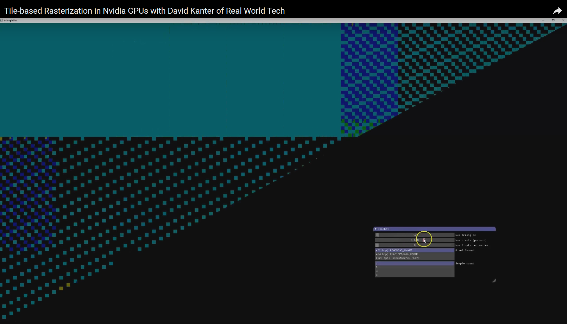
NVIDIA Maxwell Architecture Rasterization Tiling Pattern (Image Courtesy: Real World Tech)
Tile based rendering is something we’ve seen for some time in the mobile space, with both Imagination PowerVR and ARM Mali implementing it. The significance of tiling is that by splitting a scene up into tiles, tiles can be rasterized piece by piece by the GPU almost entirely on die, as opposed to the more memory (and power) intensive process of rasterizing the entire frame at once via immediate mode rendering. The trade-off with tiling, and why it’s a bit surprising to see it here, is that the PC legacy is immediate mode rendering, and this is still how most applications expect PC GPUs to work. So to implement tile based rasterization on Maxwell means that NVIDIA has found a practical means to overcome the drawbacks of the method and the potential compatibility issues.
In any case, Real Word Tech’s article goes into greater detail about what’s going on, so I won’t spoil it further. But with this information in hand, we now have a more complete picture of how Maxwell (and Pascal) work, and consequently how NVIDIA was able to improve over Kepler by so much. Finally, at this point in time Real World Tech believes that NVIDIA is the only PC GPU manufacturer to use tile based rasterization, which also helps to explain some of NVIDIA’s current advantages over Intel’s and AMD’s GPU architectures, and gives us an idea of what we may see them do in the future.
Source: Real World Tech


191 Comments
View All Comments
silverblue - Tuesday, August 2, 2016 - link
PowerVR 2 was delayed so that NEC/Videologic could manufacture enough for Dreamcast, meaning the PC launch of the Neon250 was after its competitors had caught up.The first Kyro was also horribly underclocked, requiring Kyro II to fix its shortcomings (175MHz instead of 115).
Yojimbo - Monday, August 1, 2016 - link
I wonder if AMD would have to license IP to do tile-based rendering. NVIDIA has tile-based rendering IP from Gigapixel via 3dfx. AMD sold their Imageon IP to Qualcomm whereupon it was used for Adreno.wumpus - Tuesday, August 2, 2016 - link
3dFX bought Gigapixel in 2000. Any patents applied for in the last year (how much do you think they were spending on R&D then?). If AMD starts designing a tiling chip right now, any Gigapixel patents will have safely expired before first silicon.Yojimbo - Wednesday, August 3, 2016 - link
Firstly, that's 4 more years without access to TBR (the patent term is 20 years). And 6 years since Maxwell came out. I'd bet that AMD knew quite a bit about NVIDIA's rasterization process soon after they got their hands on a GPU. I seriously doubt this public revelation told AMD anything they didn't already know. If a technique really is giving NVIDIA an advantage, they'd want to neutralize that advantage as soon as possible if they can, not wait up to 6 years.Secondly, you're making an assumption that they can do what they want with TBR with just the original Gigapixel patents. Other companies (Apple, ARM, Qualcomm, NVIDIA) have since filed for other patents dealing with TBR and if AMD has not already been researching TBR before now, they very well may need to be careful to not violate some of those patents as well as they go forward trying to apply TBR in modern architectures. So if whatever cross-patent deals they already have in place don't include TBR patents, they may need to seek new deals to safely pursue TBR.
Haroon90 - Monday, August 1, 2016 - link
AMD stated their 2018 Navi architecture will be mobile first so I presume they will implement something similar to this.Eden-K121D - Monday, August 1, 2016 - link
Source?Haroon90 - Monday, August 1, 2016 - link
My mistake they said it will be their first architecture with "scalability" in mind.What else could that mean besides mobile,their gpus already scale from servers to laptops and judging by the power efficiency gains its slated to have that can only mean it has a mobile centered design.
Yojimbo - Monday, August 1, 2016 - link
Yeah I think Navi is the next chance for AMD to be more competitive against NVIDIA. AMD hasn't been as nimble as NVIDIA and I think their GCN architecture was designed for a different world than its being used in. I would like to think Navi is a big architectural overhaul, the biggest for AMD since the original GCN came out in 2011.tarqsharq - Monday, August 1, 2016 - link
Considering AMD spends less than Nvidia on R&D, while also trying to compete with Intel on the CPU side with that same budget, the work they have done is impressive.Yojimbo - Monday, August 1, 2016 - link
Not sure how one makes an accurate judgment of such a situation. I personally have zero experience with knowing what's possible with smaller R&Ds in the semiconductor industry. I have no data to compare this situation to. But I don't find much impressive about AMD's recent GPUs. It would be impressive if they were still competitive with a lower R&D, but the fact that their market share has been cut in half makes it hard to be impressed. I have a feeling the major areas where NVIDIA spends more money than AMD might be with software and individual GPU design, and not as significantly with architecture design. When NVIDIA makes an architecture they seem to be able to apply it to their entire lineup much faster than AMD can.