Ten Year Anniversary of Core 2 Duo and Conroe: Moore’s Law is Dead, Long Live Moore’s Law
by Ian Cutress on July 27, 2016 10:30 AM EST- Posted in
- CPUs
- Intel
- Core 2 Duo
- Conroe
- ITRS
- Nostalgia
- Time To Upgrade
Looking to the Future:
International Technology Roadmap for Semiconductors 2.0
The ten year anniversary of Conroe comes at a time when the International Technology Roadmap for Semiconductors report into the next 10-15 years of the industry has been officially launched to the public. This biennial report is compiled by a group of experts in the semiconductor industry from the US, Europe and Asia and is designed to help the industry dictate which path to focus R&D for the next 10-15 years, and runs for nearly 500 pages. While we could go into extensive detail about the contents, we plan to give a brief overview here. But for people interested in the industry, it’s a great read for sure.
The report includes deep discussions regarding test equipment, process integration, radio frequency implementations (RF), microelectromechanical systems (MEMs), photolithography, factory integration, assembly, packaging, environmental issues, improving yields, modeling/simulation and emerging materials. With a focused path to a number of technologies, the hope is that leading contenders in each part of the industry can optimize and improve efficiency in directional research and development, with the possibility of collaboration, rather than taking many different routes.
Obviously such a report is going to make successful and unsuccessful predictions, even with a group of experts, based on the introduction of moonshot style features (FinFET) or unforeseen limitations in future development. For example, here is the first roadmap published by the Semiconductor Industry Association in the first report in 1993:
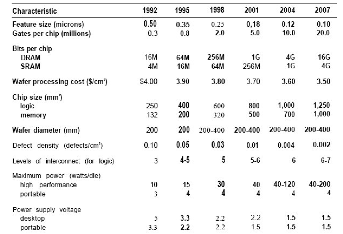
Original 1993 Semiconductor Industry Association roadmap
As we can see, by 2007 it was predicted that we would be on 10nm 100nm chips with up to 20 million ‘gates’, up to 4GB of SRAM per chip and 1250mm2 of logic per die. Up to 400mm wafers were expected in this timeframe, with 200W per die and 0.002 defects per square cm (or 5.65 errors per 300mm wafer).
Compare that to 2016, where we have 16/14nm lithography nodes running 300mm wafers producing 15 billion transistors on a 610mm2 die (NVIDIA P100). Cache currently goes up to 60-65MB on the largest chips, and the power consumption of these chips (the ASIC power) is around 250W as well. So while the predictions were a slow on the lithography node, various predictions about the integration of components onto a base processor were missed (memory controllers, chipsets, other IO).
What makes the most recent report different is that it is listed as the last report planned by ITRS, to be replaced by a more generalized roadmap for devices and systems, the IRDS as the utility of semiconductors has changed over the last decade. In this last report, a number of predictions and focal points have been picked up by the media, indicating a true end to Moore’s Law and how to progress beyond merely shrinking lithography nodes beyond 7nm. Part of this comes from the changing landscape, the move to IoT and the demand for big data processing and storage, but also the decrease in the profitability/performance gain of decreasing node sizes in comparison to their cost to develop is, if believed, set to put a paradigm shift in integrated circuit development. This applies to processors, to mobile, to DRAM and other industry focal points, such as data centers and communications.
I do want to quote one part of the paper verbatim here, as it ties into the fundamental principles of the future of semiconductor engineering:
“Moore’s Law is dead, long live Moore’s Law”
The question of how long will Moore’s Law last has been posed an infinite number of times since the 80s and every 5-10 years publications claiming the end of Moore’s Law have appeared from the most unthinkable and yet “reputedly qualified” sources. Despite these alarmist publications the trend predicted by Moore’s Law has continued unabated for the past 50 years by morphing from one scaling method to another, where one method ended the next one took over. This concept has completely eluded the comprehension of casual observes that have mistakenly interpreted the end of one scaling method as the end of Moore’s Law. As stated before, bipolar transistors were replaced by PMOS that were replaced by NMOS that were also replaced by CMOS. Equivalent scaling succeeded Geometrical Scaling when this could not longer operate and now 3D Power Scaling is taking off.
By 2020-25 device features will be reduces to a few nanometers and it will become practically impossible to reduce device dimensions any further. At first sight this consideration seems to prelude to the unavoidable end of the integrated circuit era but once again the creativity of scientists and engineers has devised a method ‘To snatch victory from the jaws of defeat’.


158 Comments
View All Comments
Icehawk - Wednesday, July 27, 2016 - link
I replaced my C2D a couple of years ago only because it needed yet another mobo and PSU and I do like shiny things, I'd bet if it was still around I could pop in my old 660GTX and run most games just fine at 1080. At work there are some C2Ds still kicking around... and a P4 w XP! Of course a lot of larger businesses have legacy gear & apps but it made me chuckle when I saw the P4.With the plateau in needed performance on the average desktop there just isn't much reason to upgrade these days other than video card if you are a gamer. Same thing with phones and tablets - why aren't iPads selling? Everyone got one and doesn't see a need to upgrade! My wife has an original iPad and it works just fine for what she uses it for so why spend $600 on a new one?
zepi - Wednesday, July 27, 2016 - link
You are not mentioning FPGA's and non-volatile memory revolution which could very well be coming soon (not just flash, but x-point and other similar stuff).Personally I see FPGAs as a clear use for all the transistors we might want to give them.
Program stuff, let it run through a compiler-profiler and let it's adaptive cloud trained AI create an optimal "core" for your most performance intensive code. This recipe is then baked together with the executable, which will get programmed near-realtime to the FPGA portion of the SOC you are using. Only to be reprogrammed when you "alt-tab" to another program.
Obviously we'll still need massively parallel "GPU" portion in chip, ASIC-blocks for H265 encode / decode with 8K 120Hz HDR support, encryption / decryption + other similar ASIC usages and 2-6 "XYZlake" CPU's. Rest of the chip will be FPGA with ever more intelligent libraries + compilers + profilers used to determine at software compile time the optimal recipe for the FPGA programming.
Not to mention the paradigm chances that non-volatile fast memory (x-point and future competitors) could bring.
wumpus - Thursday, August 4, 2016 - link
FPGAs are old hat. Granted, it might be nice if they could replace maybe half of their 6T SRAM waste (probably routing definitions, although they might get away with 4T), but certainly the look-up needs to be 6T SRAM. I'd claim that the non-volitile revolution happened in FPGAs (mainly off chip) at least 10 years ago.But at least they can take advantage of the new processes. So don't count them out.
lakerssuperman - Wednesday, July 27, 2016 - link
I'm reading this from my old Sony laptop with a Core 2 Duo and Nvidia GPU in it. With an SSD added in, the basic task performance is virtually indistinguishable from my other computers with much newer and more powerful CPU's. Granted it can get loud when under load, but the Core 2 era was still a ways away from the new mobile focused Intel we have now.I guess my basic point is that I got this laptop in 2009 and for regular browsing tasks etc, it is still more than adequate which is a testament to both the quality and longevity of the Core 2 family, but where we are with CPU power in general. Good stuff.
jeffry - Monday, August 1, 2016 - link
I agree. Got me a Sony SZ1m in 2007 (i think?), flip switched the core duo yonah with a core2duo T7200 merom. Because its 64 bit and now i can run 64 bit os and 64 bit software on it.boozed - Wednesday, July 27, 2016 - link
Funny to think that despite four process shrinks, there's been minimal power and clock improvement since then.UtilityMax - Wednesday, July 27, 2016 - link
To some of you it may sound like a surprise, but a Core2Duo desktop can still be fairly usable as a media consumption device running Windows 10. I am friends with a couple who are financially struggling graduate students. The other way, they brought an ancient Gateway PC with LCD from work, and they were wondering if they could rebuild it into a PC for their kid. The specs were 2GB of memory and Pentium E2180 CPU. I found inside of a box of ancient computer parts which I never throw away an old Radeon graphics card and a 802.11n USB adapter. I told them to buy a Core2Duo E4500 processor online because it cost just E4500. After installing Windows 10, the PC runs fairly smoothly. Good enough for web browsing and video streaming. I could even load some older games like Quake 3 and UrbanTerror 4.2 and play them with no glitch.UtilityMax - Wednesday, July 27, 2016 - link
I mean, the E4500 cost just 5 bucks..DonMiguel85 - Wednesday, July 27, 2016 - link
Still using a Core 2 Quad 9550. It bottlenecks most modern games with my GTX 960, but can still run DOOM at 60FPS.metayoshi - Wednesday, July 27, 2016 - link
Wow. Actually, just last holiday season, I replaced my parents' old P4 system (with 512 MB RAM! and 250 GB SATA Maxtor HDD!) with my old Core i7-860 since I upgraded to a system with a Core i7-4790K that I got on a black friday sale. The old 860 could definitely still run well for everyday tasks and even gaming, so it was more than good enough for my parents, but the video processing capabilities of the more recent chips are a lot better, which is the main reason I updated. Also, the single threaded performance was amazing for the 4790K, and the Dolphin emulator did not run so well on my 860, so there was that.Speaking of Core 2, though, I owned an ASUS UL30Vt with the Core 2 Duo SU7300 CPU and an Nvidia GeForce G 210M. While the weak GPU was not so great for high end gaming, the overall laptop was amazing. It was more than powerful enough for everyday tasks, and had amazing battery life. It was pretty much what every ultrabook today desires to be: sleek, slim, but powerful enough with great battery life. That laptop to me was the highlight of the Core 2 era. I was kind of sad to let it go when I upgraded to a more powerful laptop with an Ivy Bridge CPU and 640M LE GPU. I don't think any laptop I owned gave me as much satisfaction as that old Asus. Good times.