Fall IDF 2006 - Day 1: Laser FSBs, more Alan Wake, Flash in Vista & DDR3
by Anand Shimpi & Cara Hamm on September 27, 2006 3:16 AM EST- Posted in
- Trade Shows
For the first IDF after Intel's Conroe launch you have to give Intel credit, the folks are trying their best to make things interesting. Earlier today we reported on Intel's 65nm ramp, transition to 45nm, Conroe/Woodcrest shipments and upcoming quad-core solutions among other things.
We're rounding out our first day's coverage with an update from the Intel labs on Silicon Photonics, more information on multi-threaded gaming in Remedy's upcoming thriller: Alan Wake, Intel's Robson technology for notebooks and the world's first demonstration of DDR3 memory on an unannounced Intel desktop chipset.
Silicon Photonics Interconnects: Coming to a Chip Near You
For the past five years, Intel has been hard at work on building a silicon laser. Using light as a medium for data transmission is nothing new, after all many high speed networks operate over fiber optic cable, however the idea of using light as an alternative to electrical signaling at the chip level is a bit more revolutionary.
Photonic signaling is in many ways superior to electrical signaling as you can get much higher bandwidths out of an optical bus than you can out of an electrical bus. As the number of CPU cores and their operating frequencies increase tremendously, the demands for a higher speed I/O interface will as well. There will come a time where sending electrical data over copper wires is no longer fast enough to keep up with the growing bandwidth needs of these processors, and it's at that point where we'll have to turn to another, higher bandwidth solution. Intel hopes that its research into Silicon Photonics will hold the key to that solution.
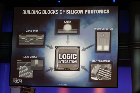
As we mentioned earlier, transmitting data using light has been around for ages, whether in the form of igniting a fire to mean "help!" or using light (or the absense of it) to represent binary data. The trick is being able to generate and use light entirely on silicon, because if you can do that, then you can use light to transmit data on die. In order to build silicon around optical interfaces you need to first be able to generate light on die itself, in other words you need to be able to generate light using electricity within the confines of a silicon chip.
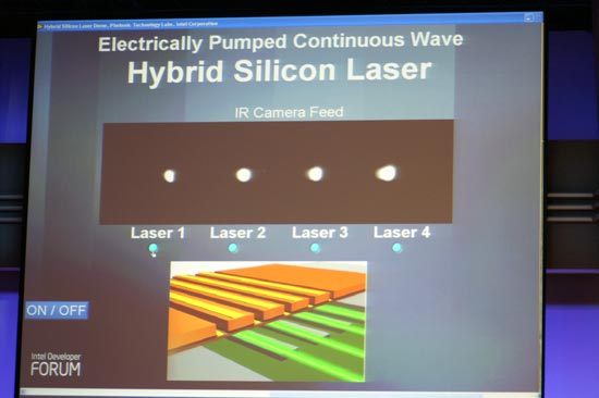
In the past, Intel's Silicon Photonics demonstrations have used externally generated light as a laser source and then worked on integrating the various other parts of the equation on silicon. Just recently, Intel demonstrated its first hybrid silicon laser that was made using standard silicon maufacturing techniques. The name hybrid silicon laser comes from the fact that the laser is produced from a combination of Indium Phosphide and standard silicon.
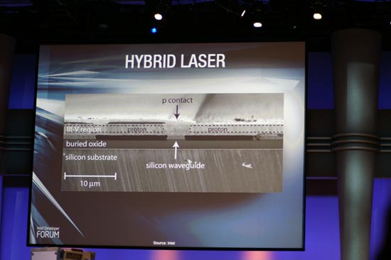
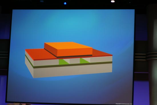
Wave guides are etched out of the silicon layer of the chip, allowing the eventual laser to be channeled, but in order to actually generate the light using electricity you need a compound that will produce light - in this case, it's Indium Phosphide (a III-V compound as it is produced using elements from the III and V columns of the periodic table).
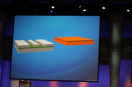
A layer of Indium Phosphide is created to be the same size as the silicon which the waveguides are carved out of.Both the silicon and InP are exposed to an oxygen plasma to create a glue-like layer, approximately 25 atoms thick, on both layers.
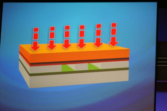
Then, the silicon and InP are fused together and channels are etched out of the top InP layer:
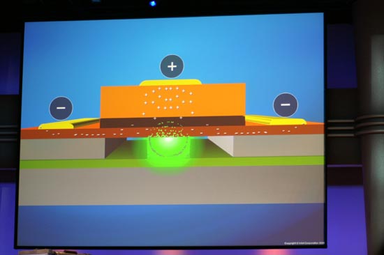
When you apply a charge across the InP layer, the electrons cause the InP to generate light that is then reflected into the waveguides in the silicon, thus creating a laser within silicon.
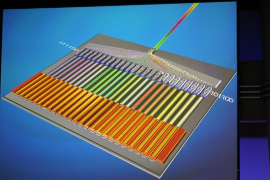
Being able to generate the laser on silicon is just one step of the whole process, but it is a very important one. With lasers generated, you can then encode binary data on and multiplex multiple lasers into a single output, offering tremendous bandwidth.
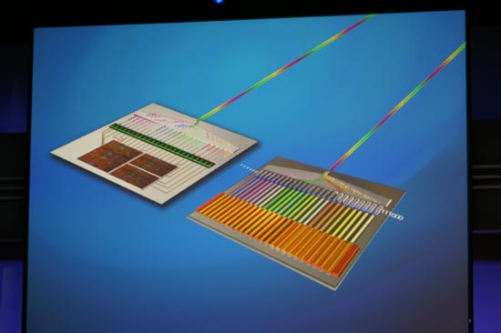
The data can then be sent over the single output to a de-multiplexer and decoder that would recover the original binary data and convert it back into electrical signals that could be used by regular silicon based processors:
Intel is still years away from being able to use any of this silicon photonics technology in a product, but progress is being made. Intel demonstrated its hybrid laser at IDF, simply showing that it works and was produced using conventional silicon manufacturing processes.
The apparatus below basically holds a hybrid laser chip, provides it with power and is placed next to an IR camera to detect the light produced by the chip:
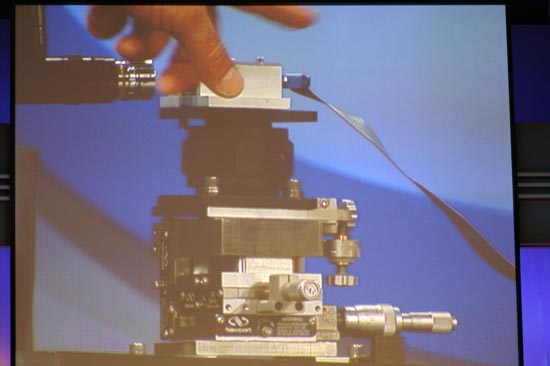
As you can see the chip does produce light, and Justin Rattner even slid his hotel keycard between the camera and the chip to confirm that the demo was live and that the chip was actually producing the light.
The implications of Intel's work in silicon photonics are tremendous, as it would allow Intel the bandwidth necessary to connect CPUs with tens or hundreds of cores to the outside world. While we're still years away from seeing this technology used in a product, we were glad to see Intel keep us updated on its progress.
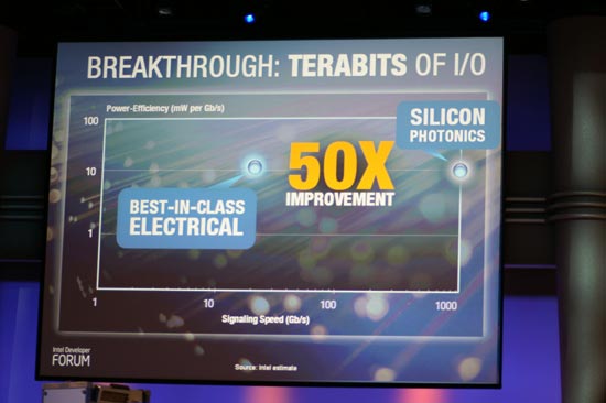
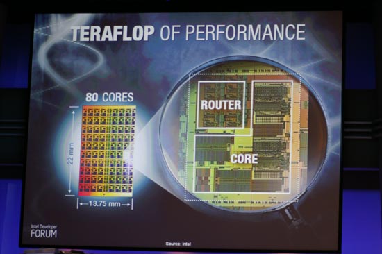
Alongside Intel's focus on silicon photonics to deliver what it is calling "Terabits of I/O", Justin Rattner also talked about being able to deliver Terabytes of bandwidth and Teraflops of performance for the future of Intel microprocessors. The Terabytes of bandwidth would come through the use of stacked die technology, which Rattner talked about at IDF six months ago. As a recap, stacked die technology could be used to create a layer of cache that would attach directly to a CPU in order to give it a very large, very high performance memory subsystem that was still quite low latency.
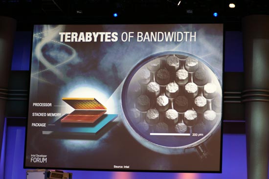
Intel's Teraflop CPU could theoretically use a stacked die approach to deliver the sort of memory bandwidth it would need to keep all 80 of its FP cores fed.


16 Comments
View All Comments
drwho9437 - Wednesday, September 27, 2006 - link
"Photonic signaling is in many ways superior to electrical signaling as you can get much higher bandwidths out of an optical bus than you can out of an electrical bus, thanks to photons traveling much faster than electrical fields."Electric signals are photons too. All EM is photons. You are just talking Giga vs Tera freq. This lets you build more ideal wave guides. But that's all. They are both apples.
stepz - Wednesday, September 27, 2006 - link
Electrical bus doesn't signal with electrons, it signals with an electrical field. Individual electrons can take several minutes to get from one pin to another. Optical bus has a bit less latency thanks to photons traveling faster than electric field (around 0.5ns less for a distance of 30cm/1 foot). It has a lot more bandwidth thanks to lack of interference and immense frequency of the carrier signal.
I assume you mean signaling at the board level. It's not practical to use optical signaling at the chip level. Wavelength of the light used is too long for widespread use as chiplevel interconnects.
Caligynemaniac2 - Thursday, September 28, 2006 - link
Actually, optical buses will have more latency than electrical buses. E&M signals propagate in copper wires at ~.9c, while fibre optic cable propagates at ~.6cFurthermore, there will be inherent latency in converting from an optical signal back to an electrical one. What you get with optical interconnects is both increased bandwidth and increased latency.
This may be offset by the ability of serial interfaces to easily revert back to parallel interfaces when coupled with optical rather than electrical signaling (i.e. it is easy to duplex optical signals and essentially impossible for electrical ones- which meant routing was a nightmare for parallel electrical signals as bandwidth needs increased, and will make routing simple for optical signals).
drwho9437 - Wednesday, September 27, 2006 - link
Its all the same all that matters for "speed" of the particle traveling is the characteristic impedance of the waveguide. Signaling bandwidth has to do with how many wiggles you can make EM fields, that is just related to the freq. Now the reason we jump to optical freq after GHz is just because there is no easy way to make the intermediate freq.JarredWalton - Wednesday, September 27, 2006 - link
Electrical fields vs. electrons... what are we, electromagnetic physicists!? ;)The point of silicon photonics is to get light down to the chip level interconnects. It's obviously not there yet. Board level signaling should already be possible, though not generally practical, and of course system level signaling has been optical for a while (server to server fibre optic connections).
VooDooAddict - Wednesday, September 27, 2006 - link
I'm already looking forward to Core 2 Quad. The news that DDR3 support is also right around the corner makes me want to wait a little longer for DDR3 and the added bandwidth and 1:1 FSB to Memory Clock.Sunrise089 - Wednesday, September 27, 2006 - link
While actually having a highly multi-threaded game will be nice, until much more specific performance info is available I see little reason why "gamers [will] start thinking about the move to dual/quad core if they haven't already."Several problems stand in the way of quad core being ideal for gaming:
1) Anandtech itself reported how difficult it was for a game developer to make their games trully multithreaded, so it remains to be seen how many games actually have the degree of threading present it Alan Wake.
2) The publisher only quoted actual performance use of the physics thread (80% of a standard clocked C2Duo), so it's VERY possible if the other threads use substantially less processing power the four cores may not be trully needed.
3) Even in this game, the publisher itsself admits that simply overclocking the dual-core machine allows for equal performance compared to the stock quad-core, so raw power seems to be trully important, not a specific number of cores.
4) The most important performance increase will always be from one core to two, since the overhead of the OS, antivirus program, etc can be removed from the primary game thread. After that, each additional core will suffer from deminished returns
5) Most importantly, going from dual to quad core costs money, and if the past is any indication, that mnoey should be better spent on a GPU upgrade. In fact, with the near theoritical doubling of performance with dual core over single, the GPU upgrade is probably reletively a better idea than it's ever been.
Until these issues are resolved I think while the game may be impressive, the idea that gamers will want to jump to quad-core is mostly marketing derived.
Anemone - Wednesday, September 27, 2006 - link
I find it disturbing that there isn't much comparison of that same Alan Wake game on a Core 2 duo. I do realize that there is a push to highlight the benefits of a quad processor, but are they now making the window for a dual core being the sweet spot to say, just 2007?See, inadvertently, they are likely smashing the sales of core 2 duo's. A lot of folks are wondering if a core 2 duo is going to be "enough" and then for how long will it be enough? Intel has built a lot of "transition" chips over the years and they often have had relatively short useful lives. Is that the reason the Core 2 duo came out so reasonably priced? Is it going to be a small one year chip that is outdated, and potentially badly so, by the end of 2007? If so, why buy one?
Some assurance would have helped a lot if we'd seen a comparison of how Alan Wake, and the benchmark quad processing programs ran on Core 2 duo's. As it is, a lot of folks are getting nervous that they have bought, or might be buying into a dead technology of "just" a dual core.
I sure hope Intel addresses this market concern before they conclude. If not, the holidays could be a very rough season for sales of Core 2 duo's.
JarredWalton - Wednesday, September 27, 2006 - link
It's IDF and Intel is pimping new technology. I would say it's pretty reasonable to assume that quad cores are not at all required. Stating that HyperThreading can run the game with lower detail is also sort of funny, as HT only gives about 10% more performance. Let's see... Athlon 64 single core 4000+ is about 20-30% faster than the best HyperThreading Pentium 4 chips, but HT is enough while a fast single core is not? I don't really buy it, although "enough" seems to be a stretch at best. I will wager that Remedy will work hard to make sure the game at least runs on single core setups, as that is still a very large market segment.Another thought: audio often uses maybe 10-20% of the CPU time in a game. So physics + audio is one core. The streaming and terrain tessellation sounds like maybe half a core at best, and the rendering would probably use the rest of the available power and then some. Remember that Xenon only has 3 cores available, all without OoO execution (Out of Order), so it's reasonable to assume 3 OoO cores will be more than enough, and in fact 2 cores is probably going to be fine.
cmdrdredd - Friday, September 29, 2006 - link
"It's IDF and Intel is pimping new technology. I would say it's pretty reasonable to assume that quad cores are not at all required. Stating that HyperThreading can run the game with lower detail is also sort of funny, as HT only gives about 10% more performance. Let's see... Athlon 64 single core 4000+ is about 20-30% faster than the best HyperThreading Pentium 4 chips, but HT is enough while a fast single core is not? I don't really buy it, although "enough" seems to be a stretch at best. I will wager that Remedy will work hard to make sure the game at least runs on single core setups, as that is still a very large market segment."This is what I think too, they would dig their own grave if they released a game that performed pitifully on a 2.6Ghz single core system. Alot of people still use those HP, and Dell systems their parent's bought them to game on (sometimes with upgraded GPU).
There's no way they can convince me that all 4 cores are needed for any game. I can see 2 because that's becomming mainstream, but to commit suicide by relegating users to abysimal performance is bad news.