Intel's 50Gbps Silicon Photonics Link: The Future of Interfaces
by Brian Klug on July 30, 2010 6:49 AM EST- Posted in
- Trade Shows
- Intel
- Photonics
- Laser
It's all about Silicon
I mentioned material constraints before - without getting into too much detail, let’s talk about what makes a laser work. For every laser, you need a few things: gain medium (which should spontaneously emit photons in the presence of other photons, effectively adding optical gain), an optical resonator or feedback (in its simplest form, a cavity with mirrors at both ends), and some way of pumping (providing energy to, either electrically, optically, or whatever works for the material) the gain medium.
The problem with silicon has been that it traditionally hasn’t lent itself to creating light very well at all - it has what’s called an indirect bandgap. When electrons fall from one energy state to the other, instead of the material emitting a photon (which is what happens in a direct bandgap material), it emits primarily phonons (lattice vibrations - and through a ton of hand waving and thermodynamic processes, heat), and very few photons. In order for a material to emit large quantities photons when electrically pumped, it should have a direct bandgap.
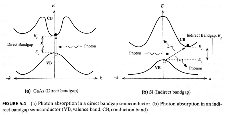
Indirect vs Direct bandgap - from Optoelectronics and Photonics: Principles and Practices by S. O. Kasap
The result for the longest time was that making a silicon laser seemed fundamentally impractical - how can something which doesn’t want to emit light be a good gain material at all?
Silicon has advantages, however. For example, silicon oxide makes an almost ideal cladding material (surrounding normal silicon). Think - fiber optic cable, but as traces embedded in your motherboard, all manufactured using traditional CMOS processes available now.
What’s new about Intel’s design - by John Bowers’ group at UCSB and a number of other researchers - is that the laser is hybrid silicon. Other previous designs have used other gain media with direct bandgaps more suitable for spontaneous emission, but with other bigger design challenges. One problem with these other materials that the crystal lattice may be too different from the silicon substrate underneath it - the result is what’s called lattice mismatch and it results in undesired optoelectronic properties. To some extent, lattice mismatch can be mitigated with an epitaxial (imagine an intermediary layer between the two mismatched material). Another problem is that thermal expansion of the materials (silicon, and whatever other material is being used for the laser) is often different as well, making it hard to physically keep things together and creating a host of other challenges. There’s also the issue of aligning the system. Previous designs have worked, at the expense of being more difficult to fabricate, and thus more expensive.

Intel’s design uses indium phosphide (InP) and aluminum gallium indium arsenide (AlGaInAs) layers, all of which can be deposited at wafer scale. The result is that there’s no discrete laser assembly or alignment. Wavelength selection and feedback are done with a distributed feedback bragg grating, which is relatively conventional. The combination of materials and manufacturing processes in this design by Intel yields itself to mass production without caveats. The end result is a hybrid silicon laser that's relatively easy to manufacture in large quantities using traditional processes.
As for the detector - bias a similar stack of components the other way, and you’re done.
Combined with Intel’s work on photonic integrated circuits on silicon for the modulator, waveguide, multiplexer and demultiplexer (for WDM), and you can see how the building blocks necessary for building optical interconnects came together.


42 Comments
View All Comments
dasHHa - Friday, July 30, 2010 - link
Moore's law still going on!Muscles - Friday, July 30, 2010 - link
A lot to look forward to in the future.DJMiggy - Friday, July 30, 2010 - link
Very good article. VERY exciting stuff. I look forward to the future. Both near and far!*sings* In the year two thousaaaaaaaaaaaaaaaaaaand!
GullLars - Wednesday, August 4, 2010 - link
*sings* In the year 2525...I just drifted off and almost drooled thinking about this combined with tiered non-uniform Solid State Storage (L1-3/4 volatile, and 4/5 none-volatile, highly parallel).
Already today you can get 100+ MB/s (read) from a single NAND chip (ONFI 2.x), so scaling out to 2^n channels you could quickly aggregate bandwidth to several GB/s for parallel workloads or bulk (>1MB) transfers, without insane costs.
With a re-make of storage management (like Fusion-IO's new "Virtual Storage Layer") and streamlining of the initiating part of program codes, you could load the operating system and any program near-instant. I've already had loading times around a second for many programs (and a few seconds for the really heavy ones) for two years now thanks to my RAIDed SSDs <3, but this would be a new level of performance.
KG Bird - Friday, July 30, 2010 - link
This was a very interesting piece and reminds me of a few things I'd stuffed into the back of my brain. Just to clear up a couple of things though...From Wikipedia: Epitaxy refers to the method of deposition a monocrystalline film on a monocrystalline substrate.
So this device is made through an epitaxial process.
Intel puts down an epitaxial buffer layer to smooth out the differences in lattices between the silicon and the next layer. If you don't use a buffer layer, you get defects such as voids or bulges that lead to the undesirable properties mentioned, or it just plain overheats at the defect location and doesn't work.
3DoubleD - Friday, July 30, 2010 - link
It is likely that the buffer layer is a metamorphic layer. The use of a quaternary alloy (AlInGaAs) alloys engineers to slowly vary the lattice constant from that of Si to that of InP. This prevents the lattice strain from ever reaching a point where it is energetically favorable to create a mismatch dislocation and thus degrading device performance. All is easier said that done and it's great that Intel was able to successfully implement this technique.Another method of integrating high performance III-V semiconductor materials onto Si are nanowires. The small nanowire diameters allows for mismatched materials to be connected without metamorphic layers.
In the next 10 years we will finally begin to leave the silicon dominated electronics industry into this hybrid type, where the superior performance of III-V semiconductors will meet the affordability and level of integration only enjoyed by the silicon community. There is no telling what this will look like, but integrated photonic circuits is just the beginning. Everything from a high mobility electron transistor to a single electron transistor would become possible on silicon in an affordable way. This will extend outside the integrated circuit world and into other areas such as solar cells, photo detectors, LEDs, biosensors, ect. We are only scratching the surface.
eanazag - Friday, July 30, 2010 - link
Good article. I am waiting for some free light Intel thingys. It happens to be 2010 now.zalves - Friday, July 30, 2010 - link
I see the future! no local storage and not even processing. Praises to the light!misterjohnnyt - Friday, July 30, 2010 - link
Maybe we can build Positronic Brains with these...Pinski - Friday, July 30, 2010 - link
So, Intel is now at 50% of what another company(Infinera) is doing. And they're doing it with 10x10Gb wavelengths. With a plan to move to 5x100Gb wavelengths by 2012.I guess, it'd be nice to have this article maybe include a comparison to what other companies are already doing or planning on doing.