Intel's 50Gbps Silicon Photonics Link: The Future of Interfaces
by Brian Klug on July 30, 2010 6:49 AM EST- Posted in
- Trade Shows
- Intel
- Photonics
- Laser
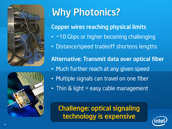
Why use light instead of copper?
High speed PCB design is already a science in and of itself. Timing requirements dictate equal path lengths for a growing number traces between components, resulting in the ever familiar squiggly designs on desktop motherboards. Higher frequencies of course also require considerations about wave propagation through the medium - just like a transmission line. At 1 GHz, for example, one wavelength is about 0.14 meters for copper traces on FR-4, one of the most common PCB materials.
There’s also propagation delay - for wires, commonly given as 1 ns for every 6 inches of length, though different media have different wave propagation speeds due to the dielectric of the medium. I could go on about the challenges of very high frequency circuit design - which I’m not an expert in by any stretch of the mind.
The end takeaway is that traditional microelectronic designs are becoming physically constrained in size with higher and higher frequencies. You physically need to have the CPU close to the memory controller, northbridge, and other components for it to work at frequencies people expect. Move it relatively far (one wavelength) away, and the design challenges start to stretch microelectronics to its limit. Ultimately, designs sacrifice speed for distance, or vice versa.
The advantages of using optical interconnects instead of traditional copper traces are numerous. Using light instead of copper promises vastly higher bandwidth, reduced latency, resistance to electromagnetic interference, and potentially even power savings.
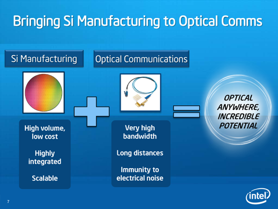
All of these reasons make using optical, silicon waveguides instead of copper traces an obvious choice. Instead of using numerous copper traces to connect the CPU to the northbridge, for example, one could envision using a single optical fiber. Or having many CPUs on one massive board connect to a chipset located even meters of path distance away. Or even have one room full of just CPUs and another room full of memory.
What Intel demonstrated on Tuesday is a working example of just that - an optical interconnect fabricated using the current traditional CMOS process, for connecting conventional electronics. Effectively an optical bus on silicon.
What’s different about Intel’s demonstration is that the lasers themselves are hybrid silicon.


42 Comments
View All Comments
dasHHa - Friday, July 30, 2010 - link
Moore's law still going on!Muscles - Friday, July 30, 2010 - link
A lot to look forward to in the future.DJMiggy - Friday, July 30, 2010 - link
Very good article. VERY exciting stuff. I look forward to the future. Both near and far!*sings* In the year two thousaaaaaaaaaaaaaaaaaaand!
GullLars - Wednesday, August 4, 2010 - link
*sings* In the year 2525...I just drifted off and almost drooled thinking about this combined with tiered non-uniform Solid State Storage (L1-3/4 volatile, and 4/5 none-volatile, highly parallel).
Already today you can get 100+ MB/s (read) from a single NAND chip (ONFI 2.x), so scaling out to 2^n channels you could quickly aggregate bandwidth to several GB/s for parallel workloads or bulk (>1MB) transfers, without insane costs.
With a re-make of storage management (like Fusion-IO's new "Virtual Storage Layer") and streamlining of the initiating part of program codes, you could load the operating system and any program near-instant. I've already had loading times around a second for many programs (and a few seconds for the really heavy ones) for two years now thanks to my RAIDed SSDs <3, but this would be a new level of performance.
KG Bird - Friday, July 30, 2010 - link
This was a very interesting piece and reminds me of a few things I'd stuffed into the back of my brain. Just to clear up a couple of things though...From Wikipedia: Epitaxy refers to the method of deposition a monocrystalline film on a monocrystalline substrate.
So this device is made through an epitaxial process.
Intel puts down an epitaxial buffer layer to smooth out the differences in lattices between the silicon and the next layer. If you don't use a buffer layer, you get defects such as voids or bulges that lead to the undesirable properties mentioned, or it just plain overheats at the defect location and doesn't work.
3DoubleD - Friday, July 30, 2010 - link
It is likely that the buffer layer is a metamorphic layer. The use of a quaternary alloy (AlInGaAs) alloys engineers to slowly vary the lattice constant from that of Si to that of InP. This prevents the lattice strain from ever reaching a point where it is energetically favorable to create a mismatch dislocation and thus degrading device performance. All is easier said that done and it's great that Intel was able to successfully implement this technique.Another method of integrating high performance III-V semiconductor materials onto Si are nanowires. The small nanowire diameters allows for mismatched materials to be connected without metamorphic layers.
In the next 10 years we will finally begin to leave the silicon dominated electronics industry into this hybrid type, where the superior performance of III-V semiconductors will meet the affordability and level of integration only enjoyed by the silicon community. There is no telling what this will look like, but integrated photonic circuits is just the beginning. Everything from a high mobility electron transistor to a single electron transistor would become possible on silicon in an affordable way. This will extend outside the integrated circuit world and into other areas such as solar cells, photo detectors, LEDs, biosensors, ect. We are only scratching the surface.
eanazag - Friday, July 30, 2010 - link
Good article. I am waiting for some free light Intel thingys. It happens to be 2010 now.zalves - Friday, July 30, 2010 - link
I see the future! no local storage and not even processing. Praises to the light!misterjohnnyt - Friday, July 30, 2010 - link
Maybe we can build Positronic Brains with these...Pinski - Friday, July 30, 2010 - link
So, Intel is now at 50% of what another company(Infinera) is doing. And they're doing it with 10x10Gb wavelengths. With a plan to move to 5x100Gb wavelengths by 2012.I guess, it'd be nice to have this article maybe include a comparison to what other companies are already doing or planning on doing.