Original Link: https://www.anandtech.com/show/2088
Fall IDF 2006 - Day 1: Laser FSBs, more Alan Wake, Flash in Vista & DDR3
by Anand Shimpi & Cara Hamm on September 27, 2006 3:16 AM EST- Posted in
- Trade Shows
For the first IDF after Intel's Conroe launch you have to give Intel credit, the folks are trying their best to make things interesting. Earlier today we reported on Intel's 65nm ramp, transition to 45nm, Conroe/Woodcrest shipments and upcoming quad-core solutions among other things.
We're rounding out our first day's coverage with an update from the Intel labs on Silicon Photonics, more information on multi-threaded gaming in Remedy's upcoming thriller: Alan Wake, Intel's Robson technology for notebooks and the world's first demonstration of DDR3 memory on an unannounced Intel desktop chipset.
Silicon Photonics Interconnects: Coming to a Chip Near You
For the past five years, Intel has been hard at work on building a silicon laser. Using light as a medium for data transmission is nothing new, after all many high speed networks operate over fiber optic cable, however the idea of using light as an alternative to electrical signaling at the chip level is a bit more revolutionary.
Photonic signaling is in many ways superior to electrical signaling as you can get much higher bandwidths out of an optical bus than you can out of an electrical bus. As the number of CPU cores and their operating frequencies increase tremendously, the demands for a higher speed I/O interface will as well. There will come a time where sending electrical data over copper wires is no longer fast enough to keep up with the growing bandwidth needs of these processors, and it's at that point where we'll have to turn to another, higher bandwidth solution. Intel hopes that its research into Silicon Photonics will hold the key to that solution.
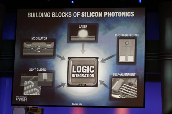
As we mentioned earlier, transmitting data using light has been around for ages, whether in the form of igniting a fire to mean "help!" or using light (or the absense of it) to represent binary data. The trick is being able to generate and use light entirely on silicon, because if you can do that, then you can use light to transmit data on die. In order to build silicon around optical interfaces you need to first be able to generate light on die itself, in other words you need to be able to generate light using electricity within the confines of a silicon chip.
In the past, Intel's Silicon Photonics demonstrations have used externally generated light as a laser source and then worked on integrating the various other parts of the equation on silicon. Just recently, Intel demonstrated its first hybrid silicon laser that was made using standard silicon maufacturing techniques. The name hybrid silicon laser comes from the fact that the laser is produced from a combination of Indium Phosphide and standard silicon.
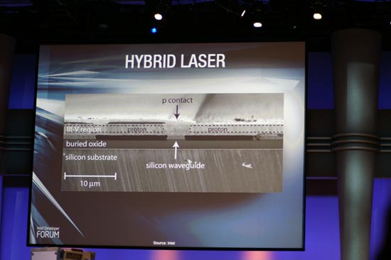
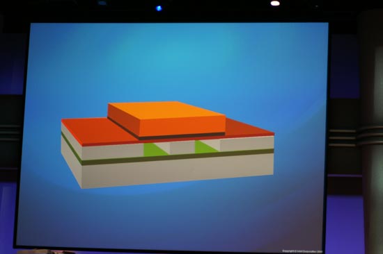
Wave guides are etched out of the silicon layer of the chip, allowing the eventual laser to be channeled, but in order to actually generate the light using electricity you need a compound that will produce light - in this case, it's Indium Phosphide (a III-V compound as it is produced using elements from the III and V columns of the periodic table).
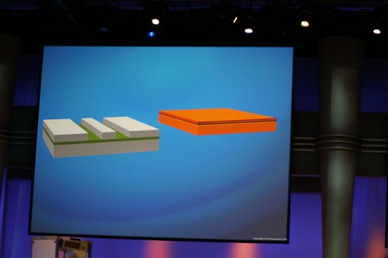
A layer of Indium Phosphide is created to be the same size as the silicon which the waveguides are carved out of.Both the silicon and InP are exposed to an oxygen plasma to create a glue-like layer, approximately 25 atoms thick, on both layers.
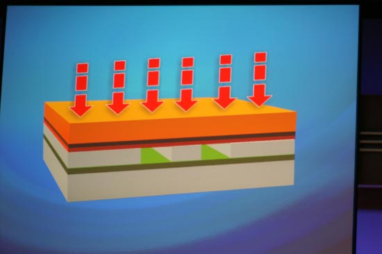
Then, the silicon and InP are fused together and channels are etched out of the top InP layer:
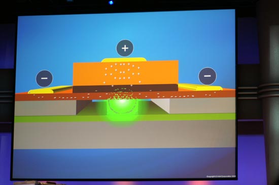
When you apply a charge across the InP layer, the electrons cause the InP to generate light that is then reflected into the waveguides in the silicon, thus creating a laser within silicon.
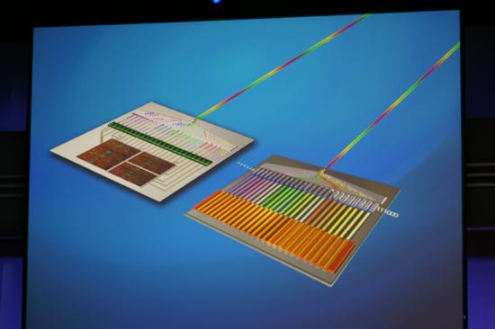
Being able to generate the laser on silicon is just one step of the whole process, but it is a very important one. With lasers generated, you can then encode binary data on and multiplex multiple lasers into a single output, offering tremendous bandwidth.
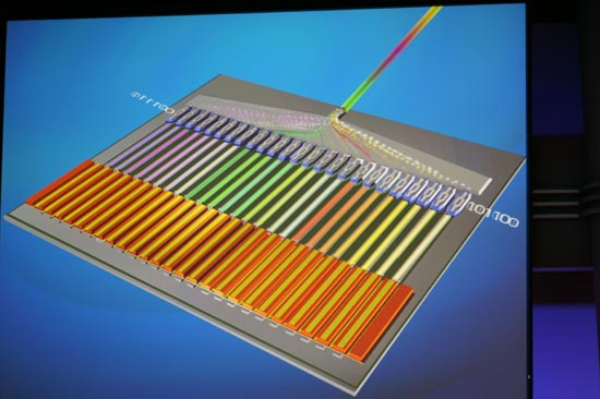
The data can then be sent over the single output to a de-multiplexer and decoder that would recover the original binary data and convert it back into electrical signals that could be used by regular silicon based processors:
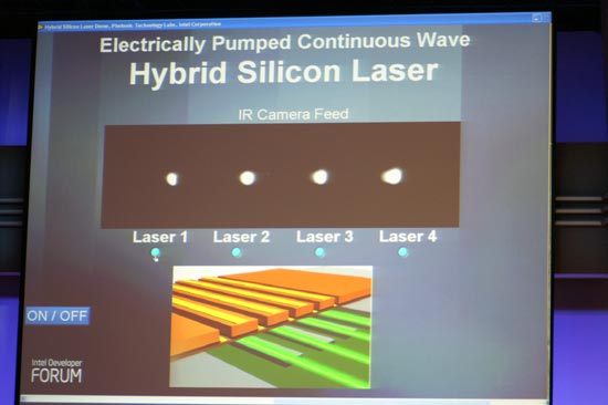
Intel is still years away from being able to use any of this silicon photonics technology in a product, but progress is being made. Intel demonstrated its hybrid laser at IDF, simply showing that it works and was produced using conventional silicon manufacturing processes.
The apparatus below basically holds a hybrid laser chip, provides it with power and is placed next to an IR camera to detect the light produced by the chip:
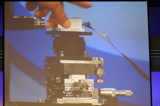
As you can see the chip does produce light, and Justin Rattner even slid his hotel keycard between the camera and the chip to confirm that the demo was live and that the chip was actually producing the light.
The implications of Intel's work in silicon photonics are tremendous, as it would allow Intel the bandwidth necessary to connect CPUs with tens or hundreds of cores to the outside world. While we're still years away from seeing this technology used in a product, we were glad to see Intel keep us updated on its progress.
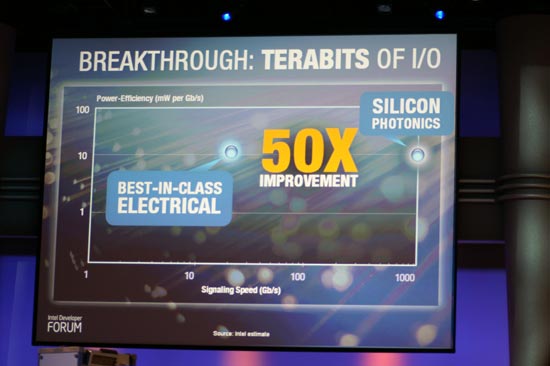
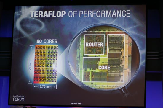
Alongside Intel's focus on silicon photonics to deliver what it is calling "Terabits of I/O", Justin Rattner also talked about being able to deliver Terabytes of bandwidth and Teraflops of performance for the future of Intel microprocessors. The Terabytes of bandwidth would come through the use of stacked die technology, which Rattner talked about at IDF six months ago. As a recap, stacked die technology could be used to create a layer of cache that would attach directly to a CPU in order to give it a very large, very high performance memory subsystem that was still quite low latency.
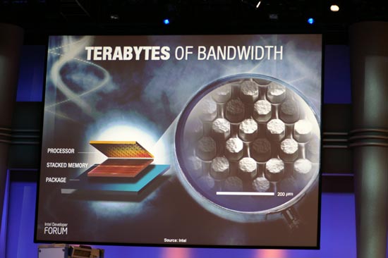
Intel's Teraflop CPU could theoretically use a stacked die approach to deliver the sort of memory bandwidth it would need to keep all 80 of its FP cores fed.
More on Alan Wake & Multi-core Gaming
We had a chance to sit down with Markus Maki and Lasse Seppanen of Remedy Entertainment, Ltd. to talk more about their upcoming psychological thriller: Alan Wake.
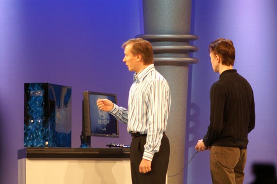
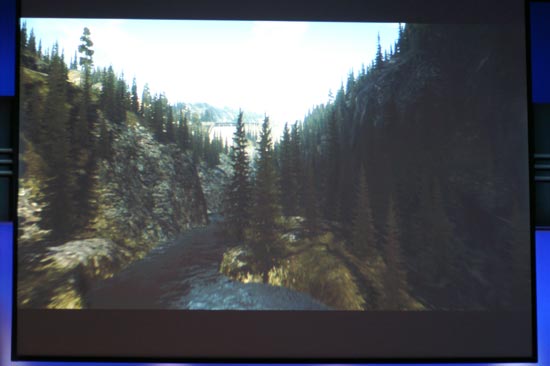
Alan Wake was demoed during Paul Otellini's keynote on an overclocked Core 2 Quad system running at 3.73GHz, mainly because the game itself is significantly multithreaded and could take advantage of the quad-core system. While development is still continuing on the forthcoming game, we did get some insight into exactly how Alan Wake will utilize multiple cores.
Surprisingly enough, Markus indicated that Alan Wake would pretty much not run on any single core processors, although it may be possible to run on single-core Pentium 4 processors with Hyper Threading enabled, with noticably reduced image quality/experience.
The game will actually spawn five independent threads: one for rendering, audio, streaming, physics and terrain tessellation. The rendering thread is the same as it would be in any game, simply preparing vertices and data to be sent to the GPU for rendering. The audio thread will obviously be used for all audio in the game, although Remedy indicates that it is far from a CPU intensive thread.
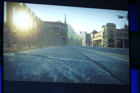
The streaming thread will be used to stream data off of the DVD or hard disk as well as decompress the data on the fly. Remedy's goal here is to have a completely seamless transition as you move from one area to the next in Alan Wake's 36 square mile environment, without loading screens/pauses. With Alan Wake being developed simultaneously for both the Xbox 360 and the PC, efficiency is quite high as developing for a console forces a developer to be much more focused than on a PC since you are given limited resources on a console. Markus admitted that being a PC-only developer can easily lead to laziness, and developing for the 360 has improved the efficiency of Alan Wake tremendously. With that said, Markus expects the visual and gameplay experience to be identical on the Xbox 360 and the PC when Alan Wake ships, hopefully without any in-game load screens.
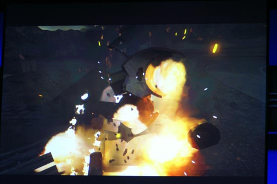
The physics thread will be used to handle all of the game's physics, which is driven using Havoc's physics engine. As Alan Wake uses Havoc's engine, there is no support for AGEIA's PhysX card and thus the host CPU must handle all physics calculations. During the keynote Markus mentioned that the physics thread used an entire core by itself, later clarifying that on a normal Core 2 Quad processor approximately 80% of one core would be used by the physics thread. With 80% of a single core being used for physics alone, the dual core CPU requirement is no longer so shocking.
As a mostly outdoor game, Alan Wake features a tremendous amount of varying terrain that is generated semi-procedurally as you encounter it. The generation/tessellation of the terrain as its encountered occupies the fifth and final thread that Remedy's game spawns. If Remedy can get the game running on Pentium 4 CPUs with HT enabled, it will be with less smooth terrain tessellation (so you may see some popping of terrain) and obviously with fewer physically simulated objects.
Although we are very curious to see how the Cell processor would run Alan Wake, given that Microsoft Game Studios is Remedy's publisher the game's Xbox 360/PC exclusivity needs no explanation. Remedy's Alan Wake team is approximately 30 strong, which is quite lean for a next-generation title, although most artwork is outsourced under the direction of Remedy. Remedy will supply specifications for the art it wants designed, and then hand it off to external art firms that will then produce it to the specs. By outsourcing the artwork, Remedy is able to focus on its development strengths and keep the overall team size down while leveraging the expertise of dedicated artists from around the world.
The demo ran extremely well on the test system, which was a Core 2 Quad running at 3.73GHz with a GeForce 7900 GTX. Markus said that it would have run just as well if the Core 2 Quad was running at its default clock speed, which we assume was 2.66GHz. The game looked even better than when we first saw it at E3 and we eagerly await its release. If Alan Wake is any indication, it won't be long before gamers start thinking about the move to dual/quad core if they haven't already.
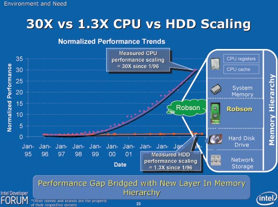
Intel Robson Technology
Intel offered some brief information on its upcoming Santa Rosa platform and its associated Robson technology:
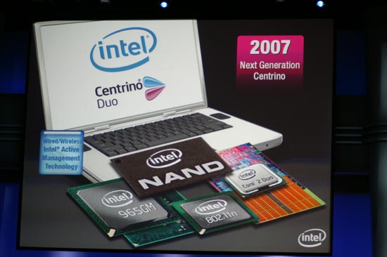
Along with 802.11n support and a new chipset (965GM), Intel's next-generation Centrino (codenamed Santa Rosa) will for the first time incorporate Intel NAND flash as a supported part of the platform. With software support from Windows Vista, Intel's Robson technology will allow notebook makers to utilize a small amount of NAND flash memory as a disk cache and/or extra virtual memory to improve performance.
Windows Vista supports two technologies that are taken advantage of by Intel's Robson (NAND flash in a notebook) technology: Windows ReadyDrive and Windows ReadyBoost.
Windows ReadyDrive is the marketing name for Vista's support for disk caching to NAND flash devices. The idea here is that ReadyDrive can cache frequently used OS and application data to a NAND flash device in order to speed up OS boot time and application load time.
Windows ReadyBoost on the other hand is designed to increase performance of systems that don't have much system memory but do have access to external flash based storage devices (e.g. USB drives). ReadyBoost will use these drives as additional virtual memory and swap to them when it runs out of main memory, which will obviously improve performance vs. simply going to disk.
ReadyBoost is really only targeted to systems with 512MB of memory that won't be upgraded (e.g. corporate desktops that you can't just stick more memory in without approval from IT), since you'd get better performance out of simply installing more memory in the system rather than relying on external flash devices as swap drives. These external flash drives have to be Vista certified in order to work with ReadyBoost (they mainly have to support a minimum read/write speed), but the performance improvement here would really only be seen on systems without sufficient main memory.
Windows ReadyDrive however can result in a significant performance increase as it acts as a cache, closing the gap between main memory and hard disk performance. Intel has been touting very tangible reductions in resume from hibernate time as well as application launch time thanks to ReadyDrive.
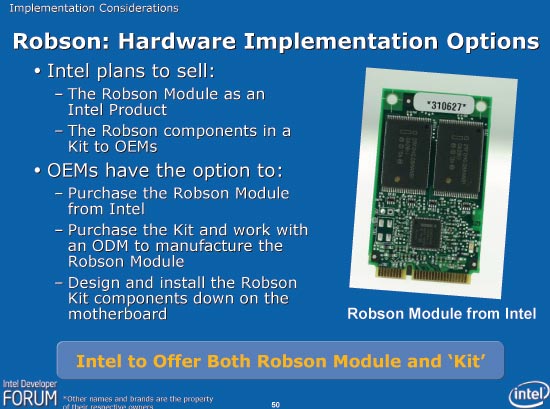
Intel's Robson technology is simply Intel's solution for both ReadyDrive and ReadyBoost; using a single Intel card (either in a Express Card slot or on the motherboard itself), Intel can support both ReadyDrive and ReadyBoost (although the latter isn't as important if you have enough main memory).
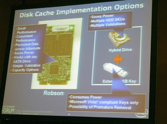
While you can take advantage of ReadyDrive with a hybrid hard drive, Intel obviously views the motherboard level integration of Robson technology as the best option.
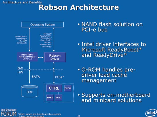
Currently Intel expects the mainstream target for Robson NAND flash to be 1GB, although higher performance alternatives would definitely be larger. In order to take advantage of both ReadyDrive and ReadyBoost, you'd have to have a Robson card equipped with two flash devices, otherwise you can only support one. Assuming it's upgradable, Intel's Robson approach makes a lot of sense since it would be a lot cheaper to simply replace a flash card in your system rather than upgrading your hard drive everytime you wanted more flash for ReadyDrive.

Although it's not a required part of the Santa Rosa platform, Intel is expecting many OEMs to take advantage of Robson technology and we will see it introduced next year alongside Vista and the new Centrino notebooks.
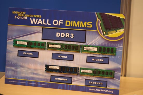
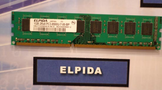
Intel Demonstrates DDR3 on Desktops
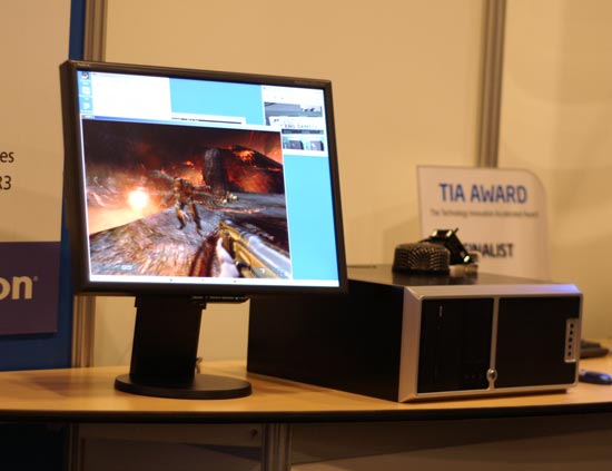
In a peculiar move, Intel is demonstrating a couple of Core 2 systems using the upcoming Bearlake chipset, due out sometime in the middle of 2007. The biggest differentiating feature between the upcoming chipset and the current solutions is official 1333MHz FSB support and DDR3 memory support:
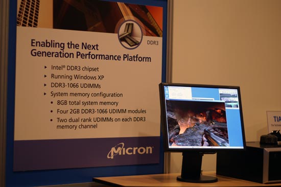
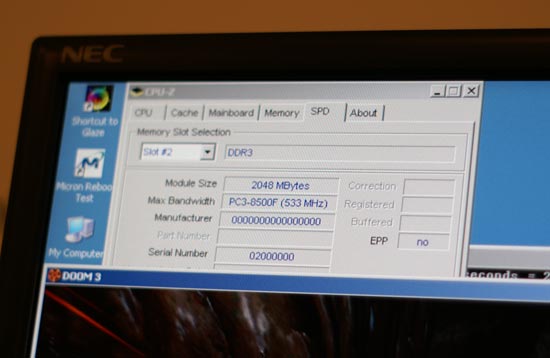
The DDR3 being used was standard 240-pin DDR3 memory running at 1066MHz (CL7). We'd expect to see DDR3-1333 by the time the Bearlake chipsets launch next year, offering a 1:1 ratio with the 1333MHz FSB.
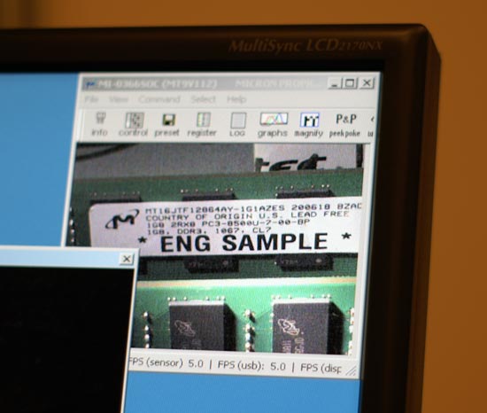
The systems were running a combination of Quake 4 (or Doom 3 depending on the system) and a modified version of CPU-Z to verify DDR3 support. Although Intel wouldn't let us peak inside the cases, there was a live webcam attached that was pointed at the DDR3 modules to remove doubt of any demo system shenanigans.
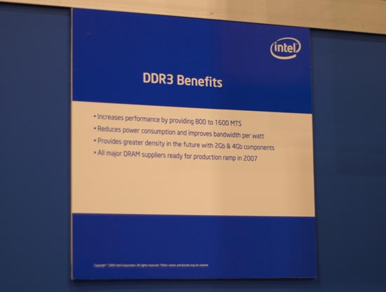
Unfortunately, lower power consumption may be the only tangible benefit users get from DDR3, as we may not see much of a performance boost since current generation DDR2 platforms aren't exactly memory bandwidth limited themselves. Hopefully Intel has learned from its mistakes with the first DDR2 chipsets and will do what it takes to make the Bearlake family of chipsets a more attractive option upon their introduction.
Final Words
Day two of the Fall Intel Developer Forum is set to begin and there's much more to talk about, we'll report it as soon as we hear it...


