Original Link: https://www.anandtech.com/show/1984
An AMD Update: Fab 36 Begins Shipments, Planning for 65nm and AM2 Performance
by Anand Lal Shimpi on April 4, 2006 11:00 AM EST- Posted in
- CPUs
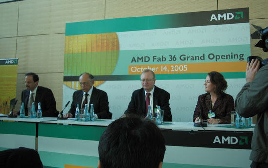
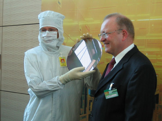
A little under 6 months ago AMD introduced their first 300mm 90nm manufacturing facility, called Fab 36. The name of course comes from its existence 36 years after the founding of AMD, with the plant itself being located next to Fab 30 in Dresden, Germany.
The grand opening of Fab 36 was mostly for media attention as the plant would not begin shipping revenue parts until Q1 of 2006. That sometime is today as AMD has just announced that Fab 36 is finally shipping revenue parts. The parts that it is shipping are 90nm Athlon 64 and Sempron CPUs, so Opterons and Athlon 64 X2s will still come out of Fab 30 next door. AMD cites customer demand as the reason that Athlon 64 and Sempron are first out of the new fab, which honestly makes sense; there's always need for more capacity at the lower end.
Although both Fab 30 and Fab 36 produce 90nm processors, Fab 30 uses smaller 200mm wafers while Fab 36 features an upgrade to 300mm wafers. AMD says that yields on 300mm wafers coming out of Fab 36 are comparable to 200mm yields being produced at Fab 30.
In terms of capacity, by 2008 AMD plans to be able to crank out 20,000 (300mm) wafers per month out of Fab 36 which would double its microprocessor production capacity to approximately 100M CPUs per year (thanks to larger wafers and smaller transistors). For comparison, Fab 30 currently produces 30,000 (200mm) wafers per month. Unfortunately AMD was unable to provide us with any sort of guidance as to how quickly Fab 36 will ramp up to its 20K per month target. AMD's partnership with Chartered Semiconductor Manufacturing Ltd. out of Singapore will guarantee additional 90nm production capacity beginning in the second half of this year. By the end of this year, AMD's capacity will have increased tremendously over the single fab they had producing 90nm parts previously.
As we mentioned in our initial coverage of Fab 36's grand opening, all parts shipping out of the plant will be 90nm, with AMD converting to 65nm starting in the second half of this year. Fab 36 will be "substantially converted" to 65nm manufacturing by the middle of 2007. Once again, AMD wasn't able to provide us with any sort of concrete details about the ramp to 65nm. It could very well be that AMD will be shipping lots of revenue generating 65nm parts by the end of this year, or they could be shipping very little. If the latter is true, then AMD's real transition to 65nm won't occur until far into 2007. When it does happen however, the move to 65nm will bring about smaller die sizes, faster switching transistors and lower power consumption for AMD, just as it has for Intel. AMD's 65nm process will incorporate their third generation of SOI technology to further reduce power consumption. AMD is promising a 40% increase in transistor performance with the move to 65nm thanks to the smaller process and the third generation SOI technology.
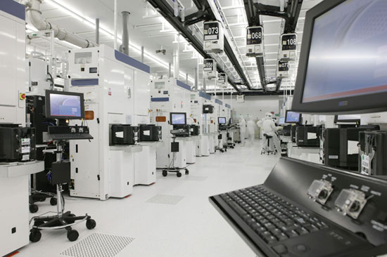
Fab 36 in Action
AMD also gave us a brief update on 45nm, stating that they have successfully produced a SRAM test wafer at 45nm. It's very popular to produce a wafer full of SRAM chips as you're bringing up and validating any new process, since the circuits are simple enough to actually make the chips producable but complex enough to get useful feedback on your process from the test wafer.
AMD's 45nm SRAM test wafer follows a little over 3 months after Intel demonstrated a similar 45nm test wafer. The benchmark when producing a wafer of SRAM is how small you're able to produce each SRAM cell. At 45nm Intel was able to achieve a 0.346 square micron SRAM cell size compared to AMD's 0.370 square micron SRAM cells. Intel's advantage in SRAM cell size is nothing new, as they have been doing so in previous process technologies as well. The advantage in SRAM cell size is one reason why you often see Intel more eager to equip its CPUs with larger L2 caches; obviously with no on-die memory controller, Intel also often benefits much more from a larger L2 cache than AMD in the first place.
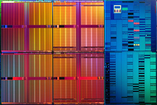
Intel's 45nm SRAM test vehicle - 0.346 sq micron cell size
Today's update had nothing to do with Socket-AM2 or AMD's transition to DDR2, but we do have some news with regards to that as well. As you've undoubtedly heard and maybe even seen elsewhere, AMD's AM2 platform has not been performing very well in development over these past couple of months. Just before IDF, AM2 samples were still performing lower than their Socket-939 counterparts, which was beginning to worry us and AMD's parters a bit. However we're excited to report that AM2 performance has finally started exceeding that of Socket-939. The performance gains we've been hearing and seeing are generally 5% or lower at the same clock speeds using DDR2-800, but it's still very early. The main point to take home is while the final verdict is still not out, AM2 is at least starting to look like more of an upgrade and not what we saw with Intel's DDR to DDR2 transition almost 2 years ago.
There's still a lot that AMD does have to give us however, including a more specific roadmap of what comes after their DDR2 transition. AMD's Phil Hester has publicly stated that once AM2 launches it will be more forthcoming with information on future architecture revisions, we can only hope so because over the past 12 months Intel has put the pressure on AMD to really start talking about the future.
The good news today is that AMD is truly growing as a company. By 2008 AMD hopes to be able to double its yearly shipments of microprocessors, and it's finally got manufacturing capacity to do just that. For the past few years AMD has held technological and performance advantages over Intel, now it's time for AMD to play catchup on the manufacturing side. AMD has a long way to go before being anywhere close to Intel's manufacturing abilities, but it is in a very good place today.


