AMD's Fab 36 Grand Opening - 90nm and 300mm in Germany
by Anand Lal Shimpi on October 14, 2005 7:50 AM EST- Posted in
- CPUs
After 24 months of construction, today AMD's first 300mm semiconductor fab, Fab 36, celebrates its grand opening. Built adjacent to AMD's 200mm Fab 30 in Dresden, Germany, Fab 36's grand opening takes place 6 years after Fab 30's introduction. The name Fab 36 comes from its existence 36 years after the founding of AMD.
The announcement for Fab 36's site in Dresden came in November 2003, with first ground breaking at the end of that month. Approximately 12 months later, the building was ready for equipment, and another 12 months after that, Fab 36 began preparations for mass production.
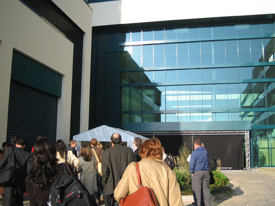
Over 150 members of the press enter AMD's press conference at Fab 36 in Dresden
Unfortunately, at its grand opening, Fab 36 is still a 90nm-only fab; throughout the next year, AMD will begin the transition to 65nm production. The first CPUs built at Fab 36 will be shipping in the first quarter of 2006, with the first 65nm chips leaving Fab 36 by the end of 2006.
Sometime in 2007 AMD will have performed a "substantial amount" of the transition of Fab 36 to a 65nm semiconductor fab, bringing the grand total for the cost of Fab 36 to an astounding 2.5 billion US dollars. There is no word when Fab 36 will be completely converted to 65nm manufacturing.
By 2008, Fab 36 will be able to produce more than 2x the number of processors as Fab 30 (potentially 100M processors per year based on current die sizes).
The first 300mm wafer produced at Fab 36 actually took place back in March, but preparation for mass production continues up to and beyond today. Today's grand opening of Fab 36 marks a huge step in AMD history, as it will hopefully alleviate a number of the supply issues they have been plagued with in recent history.
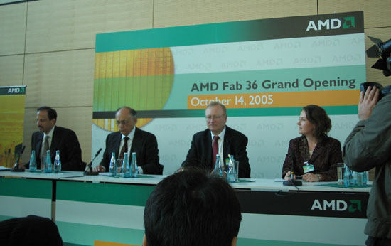
The two individuals in the middle kicked off the day at Fab 36, AMD's CEO, Dr. Hector Ruiz is the second on the left, and VP/GM of AMD Dresden, Dr. Hans Deppe is to the right of Dr. Ruiz.
The day started off with a press conference kicking off the grand opening of the fab. Below we've got a picture of a clean room engineer (or someone dressed as one) posing with AMD's Dr. Hans Deppe, the Corporate VP and General Manager of AMD in Dresden.
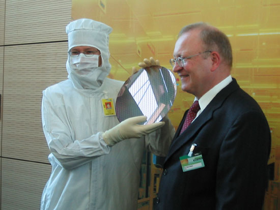
While we don't have a 200mm wafer here to compare sizes with, imagine the wafer pictured above, but smaller.
After some brief words about the opening of Fab 36, a brief Q&A period started. One of the first questions was what will happen to Fab 30 in the future now that Fab 36 is ready to start mass production. Dr. Ruiz mentioned that Fab 30 could be used for more x86 microprocessor production, it could potentially become a chipset manufacturing fab (possibly indicating AMD's intentions to eventually return to chipset manufacturing), or it could be upgraded to future semiconductor technologies for use in the future (e.g. 65nm).
One other important question that was asked was "why Dresden" for Fab 36, to which the answer was obviously multi-faceted:
1) First and foremost, AMD has invested a lot in the people of Dresden, when it comes to training and expertise in semiconductor manufacturing. It was simply easier to leverage the existing human investment.
2) Obviously government subsidies played a large role in AMD's decision to bring Fab 36 to Dresden. Dr. Hans Deppe listed the total amount of government subsidies for Fab 36 as 500 million US dollars.
The final question of the press conference was about AMD's future fab plans, which Dr. Ruiz answered with a timeframe of 2008 for the start of production on the next major fab plant.


70 Comments
View All Comments
cryptonomicon - Saturday, October 15, 2005 - link
how exciting :Di always wanted AMD to get a new fab, what takes em so long :P
rcc - Friday, October 14, 2005 - link
that a company suing someone else for business practice and unfair competition can annouce that it got a half billion dollar of government subsidizing on a new Fab plant without anyone commenting on it. So I had to. : )eljefe2 - Friday, October 14, 2005 - link
If you live in the US, yes this would be an issue. However they live in Germany. they have a socialist and MUCH more advanced society for handling the big business to employee gap. The corporation, as originally designed by Alexander Hamilton, was an entity of the public that is meant to serve the public and if it does not, it cannot exist. They in germany really see things like this. the pride of the worker ='s the pride of the nation ='s the pride of a company.would be nice.
phantom505 - Friday, October 14, 2005 - link
What about SOI? As far as I know Intel never implemented it.So how do you figure AMD is a year behind Intel when they went VERY different strategies and routes?
Spoonbender - Monday, October 17, 2005 - link
Because AMD is going to have 65nm a year after Intel. Simple as that. Yes, of course they both have some different technologies, but a 90nm chip has a bigger die area than an equivalent 65nm chip. That means a 90nm chip is more expensive to produce, because there's room for fewer chips per wafer.What you might have missed is that this isn't a question of performance. AMD is not behind Intel at all when it comes to making good, fast CPU's.
They are behind when it comes to producing them as cheap as possibly. Because they won't be able to shrink to 65nm until a year after Intel.
fishbits - Friday, October 14, 2005 - link
Heheheh. Geeks. Was this accompanied by "Thus Spake Zarathustra?"
Anyhow, congrats to AMD and Germany, great news.
Questar - Friday, October 14, 2005 - link
I think it would be better news if it was AMD and the US.mlittl3 - Friday, October 14, 2005 - link
Uh, the US is the most economical strong country in the world. Stop being such a stupid patriot and realize that all people of the world benefit when any one country benefits from technological innovation. Man, we really need to get Americans to shutup and stop being so greedy.By the way, I'm an American. :)
overclockingoodness - Friday, October 14, 2005 - link
Actually, it's better AMD didn't open a Fab in the U.S. They would have to pay much higher wages, taxes etc.By opening a fab in Germany, they will hopefully save that money to expand (notice I didn't say they will pass on the savings to its customers, which would never happen) and they need this money if they want to start construction of a new fab plant in 2008.
eljefe2 - Friday, October 14, 2005 - link
higher wages???have you seen the european euro vs us dollar? its really destroying us. (us the um, US) East germany does actually have lower wages than we do. However, they have amazing schools over there all free, all health care free, 1 month paid leave a year, free child care.... The amount the corporations actually pay per person is very high. I think they just put this plant there because, as the article notes, the people there are very good workers and very knowledgable. not ever corporation follows the juvenile philosophy of "give it to a pathetic third world nation and see what profits we can make". It is good to see that. After all, 27% of US population are direct descendents from Germany. More than any other culture percentage wise. The better europe does, the more the structure of corporations are bent to a first world society vs a 10 cents an hour slave labor force structure. THis is good for all who live in the western world.