Intel Broadwell Architecture Preview: A Glimpse into Core M
by Ryan Smith on August 11, 2014 12:01 PM ESTBroadwell CPU Architecture
We’ll kick off our look at Broadwell-Y with Broadwell’s CPU architecture. As this is a preview Intel isn’t telling us a great deal about the CPU at this time, but they have given us limited information about Broadwell’s architectural changes and what to expect for performance as a result.
With Broadwell Intel is at the beginning of the next cycle of their tick-tock cadence. Whereas tock products such as Haswell and Sandy Bridge designed to be the second generation of products to use a process node and as a result are focused on architectural changes, tick products such as Ivy Bridge and now Broadwell are the first generation of products on a new process node and derive much (but not all) of their advantage from manufacturing process improvements. Over the years Intel has wavered on just what a tick should contain – it’s always more than simply porting an architecture to a new process node – but at the end of the day Broadwell is clearly derived from Haswell and will be taking limited liberties in improving CPU performance as a result.
| Intel's Tick-Tock Cadence | |||||
| Microarchitecture | Process Node | Tick or Tock | Release Year | ||
| Conroe/Merom | 65nm | Tock | 2006 | ||
| Penryn | 45nm | Tick | 2007 | ||
| Nehalem | 45nm | Tock | 2008 | ||
| Westmere | 32nm | Tick | 2010 | ||
| Sandy Bridge | 32nm | Tock | 2011 | ||
| Ivy Bridge | 22nm | Tick | 2012 | ||
| Haswell | 22nm | Tock | 2013 | ||
| Broadwell | 14nm | Tick | 2014 | ||
| Skylake | 14nm | Tock | 2015 | ||
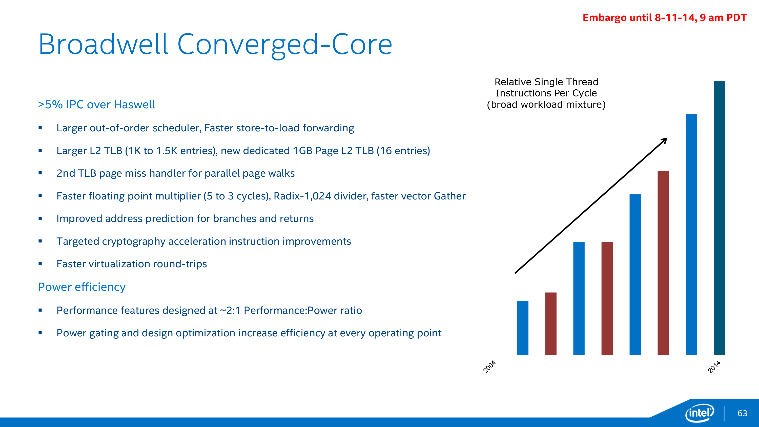
All told, Intel is shooting for a better than 5% IPC improvement over Haswell. This is similar to Ivy Bridge (4%-6%), though at this stage in the game Intel is not talking about expected clockspeeds or the resulting overall performance improvement. Intel has made it clear that they don’t regress on clockspeeds, but beyond that we’ll have to wait for further product details later this year to see how clockspeeds will compare.
To accomplish this IPC increase Intel will be relying on a number of architectural tweaks in Broadwell. Chief among these are bigger schedulers and buffers in order to better feed the CPU cores themselves. Broadwell’s out-of-order scheduling window for example is being increased to allow for more instructions to be reordered, thereby improving IPC. Meanwhile the L2 translation lookaside buffer (TLB) is being increased from 1K to 1.5K entries to reduce address translation misses.
The TLBs are also receiving some broader feature enhancements that should again improve performance. A second miss handler is being added for TLB pages, allowing Broadwell to utilize both handlers at once to walk memory pages in parallel. Otherwise the inclusion of a 1GB page mode should pay off particularly well for servers, granting Broadwell the ability to handle these very large pages on top of its existing 2MB and 4K pages.
Meanwhile, as is often the case Intel is once again iterating on their branch predictor to cut down on missed branches and unnecessary memory operations. Broadwell’s branch predictor will see its address prediction improved for both branches and returns, allowing for more accurate speculation of impending branching operations.
Of course efficiency increases can only take you so far, so along with the above changes Intel is also making some more fundamental improvements to Broadwell’s math performance. Both multiplication and division are receiving a performance boost thanks to performance improvements in their respective hardware. Floating point multiplication is seeing a sizable reduction in instruction latency from 5 cycles to 3 cycles, and meanwhile division performance is being improved by the use of an even larger Radix-1024 (10bit) divider. Even vector operations will see some improvements here, with Broadwell implementing a faster version of the vector Gather instruction.
Finally, while it’s not clear whether these will be part of AES-NI or another instruction subset entirely, Intel is once again targeting cryptography for further improvements. To that end Broadwell will bring with it improvements to multiple cryptography instructions.
Meanwhile it’s interesting to note that in keeping with Intel’s power goals for Broadwell, throughout all of this Intel put strict power efficiency requirements in place for any architecture changes. Whereas Haswell was roughly a 1:1 ratio of performance to power – a 1% increase in performance could cost no more than a 1% increase in power consumption – Broadwell’s architecture improvements were required to be at 2:1. While a 2:1 mandate is not new – Intel had one in place for Nehalem too – at the point even on the best of days meaningful IPC improvements are hard to come by at 1:1, never mind 2:1. The end result no doubt limited what performance optimizations Intel could integrate into Broadwell’s design, but it also functionally reduces power requirements for any given performance level, furthering Intel’s goals in getting Core performance in a mobile device. In the case of Broadwell this means Broadwell’s roughly 5% performance improvement comes at a cost of just a 2.5% increase in immediate power consumption.
With that said, Intel has also continued to make further power optimizations to the entire Broadwell architecture, many of which will be applicable not just to Core M but to all future Broadwell products. Broadwell will see further power gating improvements to better shut off parts of the CPU that are not in use, and more generalized design optimizations have been made to reduce power consumption of various blocks as is appropriate. These optimizations coupled with power efficiency gains from the 14nm process are a big part of the driving force in improving Intel’s power efficiency for Core M.


158 Comments
View All Comments
psyq321 - Tuesday, August 12, 2014 - link
I also fail to see how will Intel be able to keep their cadence with Skylake without either skipping the entire generation (obsoleting it in 6 months does not sound reasonable from the financial point of view) or delaying the Skylake introduction.Also the fact that Intel decided to enable all 18 cores in the Haswell EP is telling IMHO. Initially, this was to happen only with BDW-EP, so it might not be impossible that Intel might just skip Broadwell for some segments and go with Skylake.
isa - Tuesday, August 12, 2014 - link
Those who know ain't talking, but I can observe the following;- Delaying Skylake for financial reasons related to Broadwell is braindead. Broadwell development costs are sunk costs and Intel is or should be trying to maximize overall profits, not just a particular program's profits. Intel should release Skylake as quickly as possible when its yields hit target values, regardless of Broadwell delays, with two caveats:
- If the Broadwell yield difficulties also slowed down Skylake, then Skylake will likely be inherently delayed to some degree
- If Intel screws up product planning such that they flood the market with Broadwell, then their customers might be very angry if they are stuck with that inventory upon a Skylake release.
My bet at this point? Broadwell H mobile will be a very short-lived product (about 6 months).
Krysto - Tuesday, August 12, 2014 - link
Definitely not Y or U, and wouldn't get M either. Whatever is above that.mczak - Monday, August 11, 2014 - link
For the gpu It is noteworthy that unlike nvidia and amd the subslice block (at least before gen8) doesn't really have an inherent minimal size which cannot be changed without significantly altering the architecture. E.g. Gen7 (which is just about the same as Gen7.5) had subslice sizes of 6 (IvyBridge GT1), 8 (IvyBridge GT2) and 4 even (BayTrail).It is also quite interesting that everybody (nvidia since gk2xx and Maxwell, amd since even before GCN, notably their Northern Islands VLIW4 designs, intel since Gen8) now has ended up with the exact same ALU:TEX ratio (one quad tmu per 64 ALU lanes), though of course the capabilities of these tmus vary a bit (e.g. nvidia can do fullspeed fp16 filtering, amd only half speed etc.)
tuxRoller - Monday, August 11, 2014 - link
http://www.phoronix.com/scan.php?page=article&...In the fourth to last paragraph an intel driver dev says that broadwell graphics "dwarf any other silicon iteration during my tenure, and certainly can compete with the likes of the gen3->gen4 changes."
I'm going to go with the guy who's actually developing the drivers on this.
AnnonymousCoward - Tuesday, August 12, 2014 - link
Simple question: will all the new Intel desktop CPUs have integrated graphics? If the answer's yes, why would they waste the silicon area for those using discrete?name99 - Tuesday, August 12, 2014 - link
Because the people who obsess about discrete graphics are a RIDICULOUSLY small fraction of the purchasing public, a fraction which is utterly unwilling to accept this fact and the fact that CPU design is not targeted at the needs of high-end gamers.wintermute000 - Tuesday, August 12, 2014 - link
"Because the people who obsess about discrete graphics are a RIDICULOUSLY small fraction of the purchasing public"Maybe not obsess, but to characterise the PC gaming market as ridiculously small, is pretty far off the mark....
DanNeely - Tuesday, August 12, 2014 - link
Compared to the total Intel CPU market and compared to the cost of creating an IGPless CPU die for the mainstream socket it's entirely on the mark. If you want an IGPless design your only choice is to wait a year for the Xeon derived LGA2011 model; and the fact that LGA1366 launched as an enthusiast design well before the Xeon's did, but that Intel hasn't done the same for any other models shows that it didn't sell well enough to justify rushing one for us.C'DaleRider - Tuesday, August 12, 2014 - link
Small fraction is right. Projected worldwide PC hardware sales for 2015 is ~ $385B (Source: eTForcasts). Projected PC gaming sales (both hardware and software) is ~$20B (Source: Statista), less than 10% of total PC hardware sales alone. A 10% market niche is very, very small in the overall scheme of the PC market.