Intel Broadwell Architecture Preview: A Glimpse into Core M
by Ryan Smith on August 11, 2014 12:01 PM EST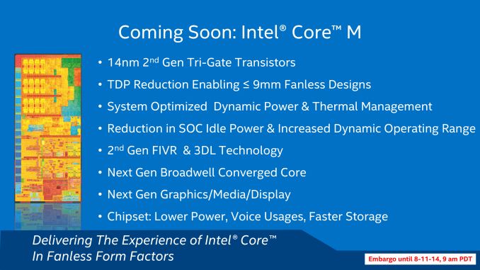
With Haswell Refresh fully behind us and 2014 now in to its second half, Intel is turning their attention to their next generation of products and processes. Intel’s tick-tock methodology coupled with the long development periods of new products means that the company has several projects in flight at any given time. So while we have seen the name Broadwell on Intel’s roadmaps for some time now, the reality of the situation is that we know relatively little about Intel’s next generation architecture and the 14nm process that it is the launch vehicle for.
Typically we would see Intel unveil the bulk of the technical details of their forthcoming products at their annual Intel Developer Forum, and with the next IDF scheduled for the week of September 9th we’ll see just that. However today Intel will be breaking from their established standards a bit by not waiting until IDF to deliver everything at once. In a presentation coinciding with today’s embargo, dubbed Advancing Moore’s Law in 2014, Intel will be offering a preview of sorts for Broadwell while detailing their 14nm process.
Today’s preview and Intel’s associated presentation are going to be based around the forthcoming Intel Core M microprocessor, using the Broadwell configuration otherwise known at Broadwell-Y. The reason for this is a culmination of several factors, and in all honesty it’s probably driven as much by investor relations as it is consumer/enthusiast relations, as Intel would like to convince consumer and investor alike that they are on the right path to take control of the mobile/tablet market through superior products, superior technology, and superior manufacturing. Hence today’s preview will be focused on the part and the market Intel feels is the most competitive and most at risk for the next cycle: the mobile market that Core M will be competing in.
To that end Intel’s preview is very much a preview; we will see bits and pieces of Broadwell’s CPU architecture, GPU architecture, and packaging, along with information about Intel’s 14nm process. However this isn’t a full architecture preview or a full process breakdown. Both of those will have to wait for Intel’s usual forum of IDF.
Diving into matters then, Core M will be launch vehicle for Broadwell and will be released for the holiday period this year. In fact Intel is already in volume production of the Broadwell-Y CPU and production units are shipping to Intel’s customers (the OEMs) to begin production and stockpiling of finished devices for the holiday launch.
Intel’s decision to initially focus Broadwell on the mobile market comes as the company takes the next step in their plan to extend into the Core processor series into these devices. Arguably, Intel has been slow to response to the rise of ARM devices, whose rapid rise has undercut traditional PC sales and quickly become the biggest threat to Intel’s processor dominance in some number of years. Intel is far from doomed right now, but even they see the potential farther down the line if they do not act.
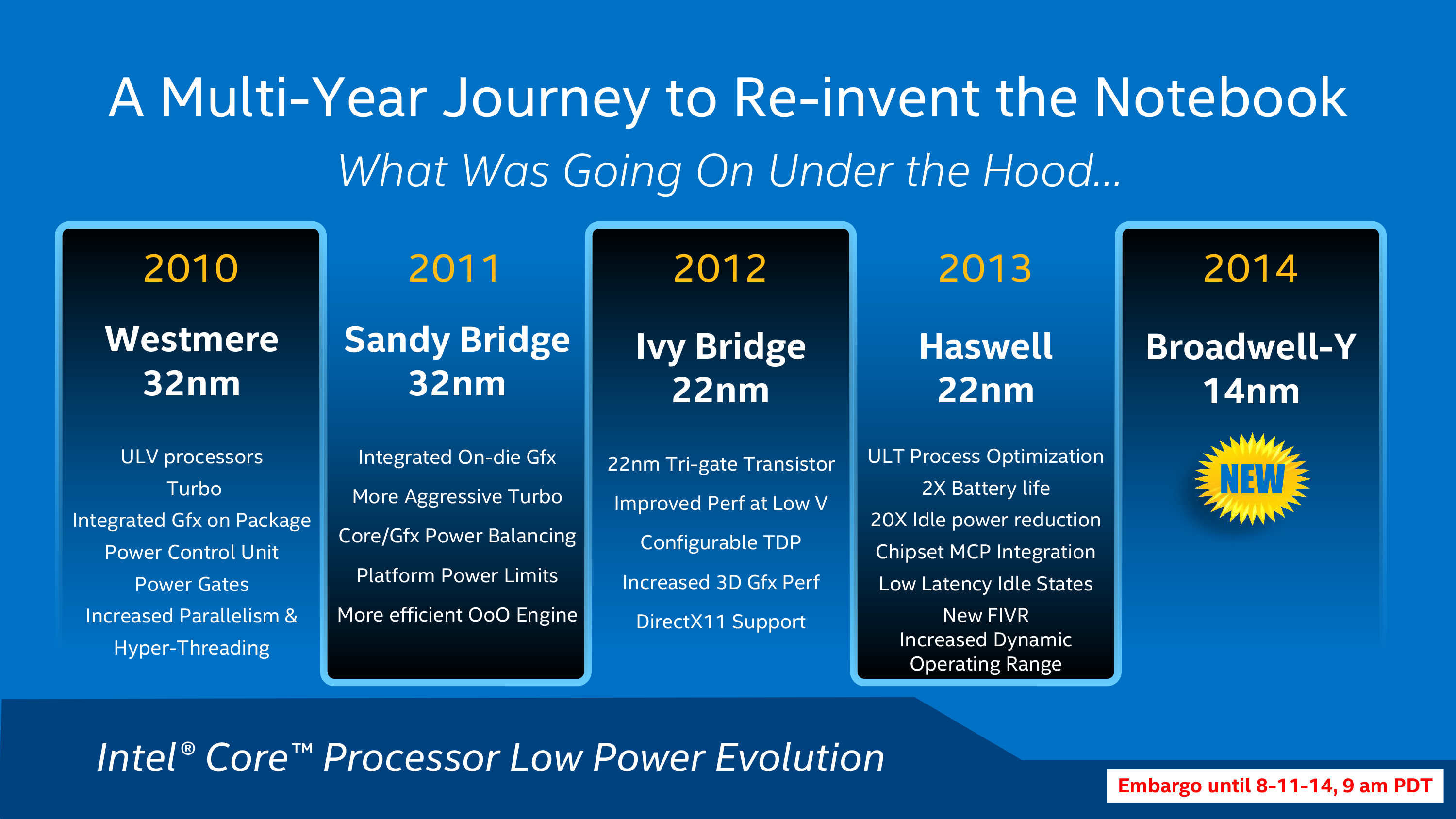
Intel for their part has responded, but it has taken a step-by-step (multi-year) process that has seen the company progressively build smaller and less power hungry CPUs in order to fit the needs of the mobile market. Since Intel integrated their graphics on-die with Sandy Bridge in 2011, the company has continued to tweak the designs of their products, with Ivy Bridge and Haswell generation products introducing further optimizations and new manufacturing processes. Now on their latest iteration with Broadwell, the company believes they’re turning a corner and have the technology they need to be a leader in the high performance mobile market. It's important to note that despite Intel's best intentions here, Broadwell and Core M remain targeted at premium devices. You won't see these parts in cheap tablets. The duty of doing battle with ARM remains Atom's alone.
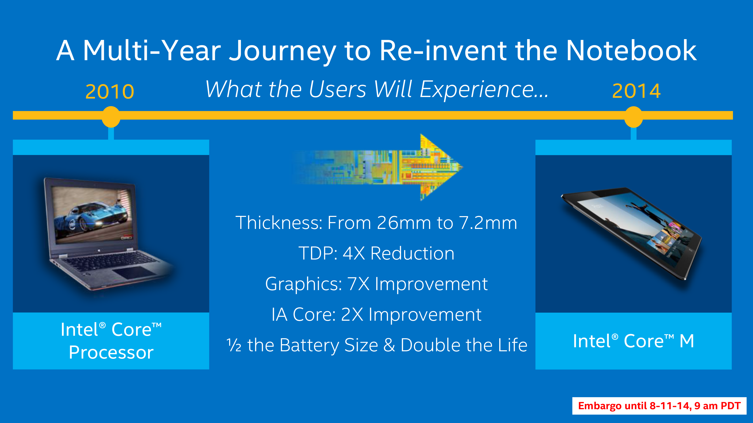
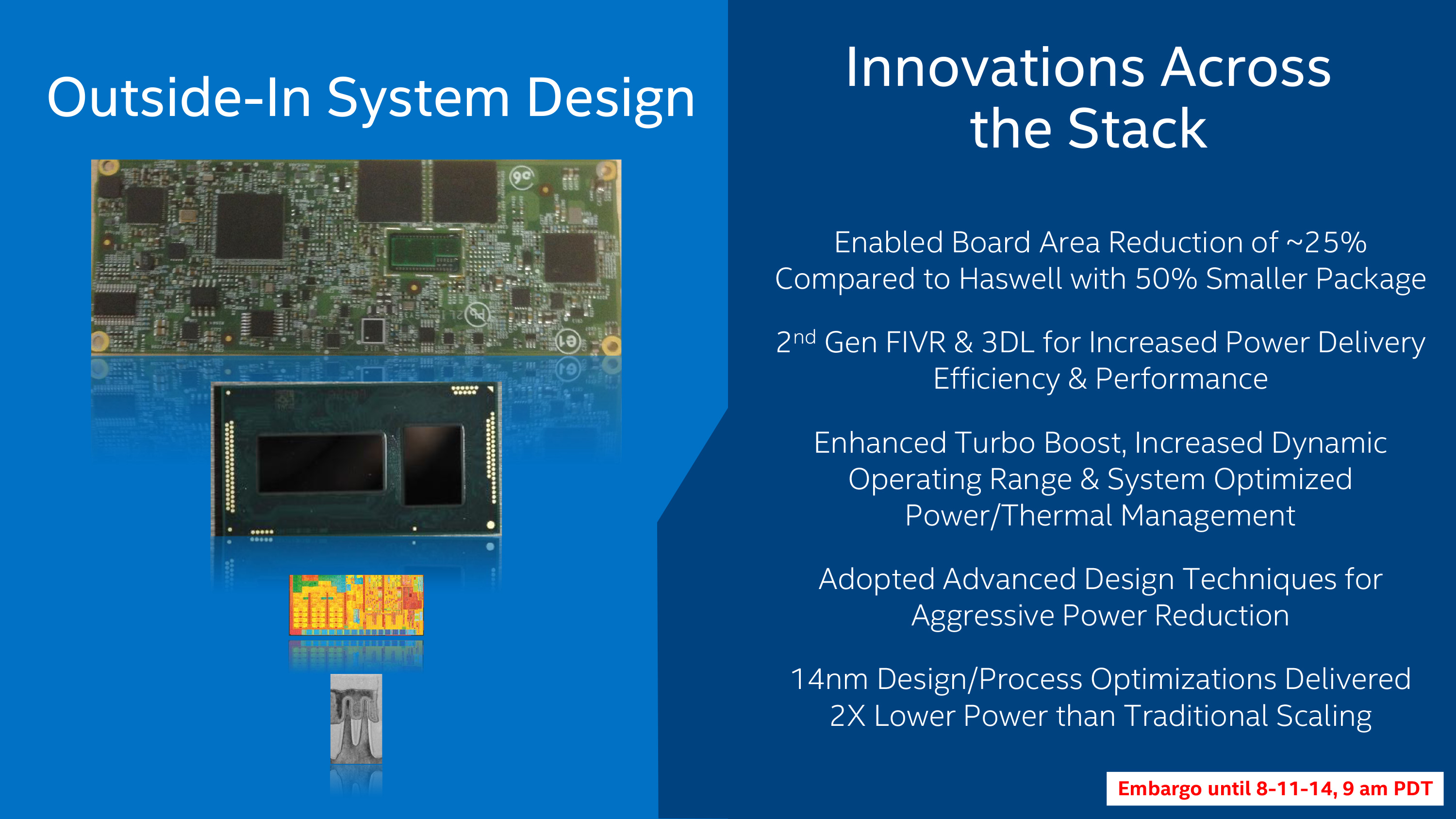
Many of these changes ultimately amount to boosting performance and reducing power consumption to a point where power and heat are where they need to be for mobile form factors, either through process efficiency improvements or through better power management and wider dynamic ranges – boosting where it matters and doing a better job of idling between tasks. However as Intel has discovered they not only need to be able to meet the TDP requirements of a tablet but they need to be able to meet the size requirements too. A particularly daunting task when the entire thickness of a device needs to be under 10mm, and the CPU thinner yet.
As a result, coupled with Core M’s performance improvements and power reductions is a strong emphasis on the size of the processor package itself and what Intel could do to reduce it. Intel calls this an outside-in system design, with various parts of Intel focusing on everything from the size of the logic board needed to hold the processor to the thickness of the processor die itself. In the following pages we’ll take a look at Intel’s efforts to get slim, but to kick things off we have a picture of Broadwell-Y from Computex 2014.
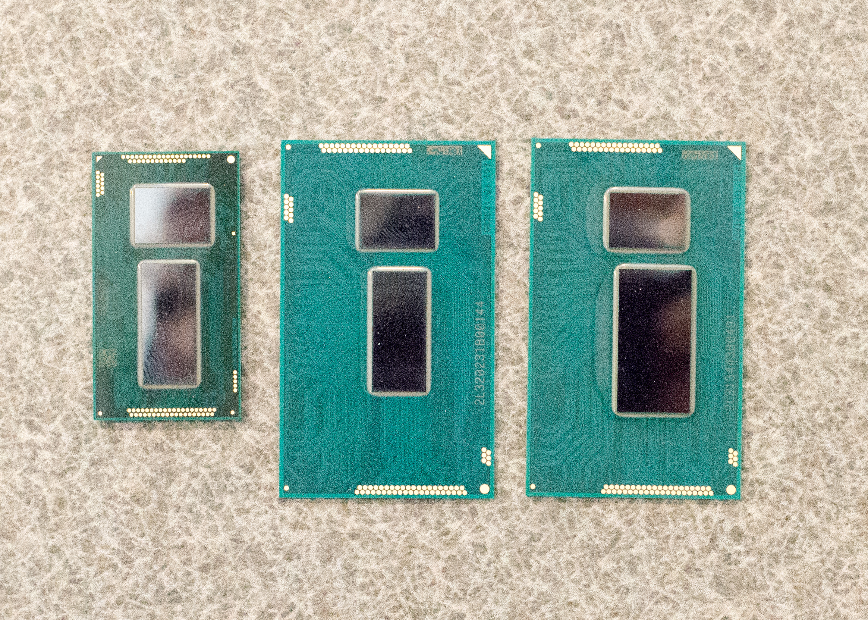
From left to right: Broadwell-Y (Core M), Broadwell ULT/ULX and Haswell ULT/ULX
Intel wants a greater foothold in the mobile market and they want it badly. And with Broadwell-Y they believe they finally have what they need to accomplish that goal.


158 Comments
View All Comments
psyq321 - Tuesday, August 12, 2014 - link
I also fail to see how will Intel be able to keep their cadence with Skylake without either skipping the entire generation (obsoleting it in 6 months does not sound reasonable from the financial point of view) or delaying the Skylake introduction.Also the fact that Intel decided to enable all 18 cores in the Haswell EP is telling IMHO. Initially, this was to happen only with BDW-EP, so it might not be impossible that Intel might just skip Broadwell for some segments and go with Skylake.
isa - Tuesday, August 12, 2014 - link
Those who know ain't talking, but I can observe the following;- Delaying Skylake for financial reasons related to Broadwell is braindead. Broadwell development costs are sunk costs and Intel is or should be trying to maximize overall profits, not just a particular program's profits. Intel should release Skylake as quickly as possible when its yields hit target values, regardless of Broadwell delays, with two caveats:
- If the Broadwell yield difficulties also slowed down Skylake, then Skylake will likely be inherently delayed to some degree
- If Intel screws up product planning such that they flood the market with Broadwell, then their customers might be very angry if they are stuck with that inventory upon a Skylake release.
My bet at this point? Broadwell H mobile will be a very short-lived product (about 6 months).
Krysto - Tuesday, August 12, 2014 - link
Definitely not Y or U, and wouldn't get M either. Whatever is above that.mczak - Monday, August 11, 2014 - link
For the gpu It is noteworthy that unlike nvidia and amd the subslice block (at least before gen8) doesn't really have an inherent minimal size which cannot be changed without significantly altering the architecture. E.g. Gen7 (which is just about the same as Gen7.5) had subslice sizes of 6 (IvyBridge GT1), 8 (IvyBridge GT2) and 4 even (BayTrail).It is also quite interesting that everybody (nvidia since gk2xx and Maxwell, amd since even before GCN, notably their Northern Islands VLIW4 designs, intel since Gen8) now has ended up with the exact same ALU:TEX ratio (one quad tmu per 64 ALU lanes), though of course the capabilities of these tmus vary a bit (e.g. nvidia can do fullspeed fp16 filtering, amd only half speed etc.)
tuxRoller - Monday, August 11, 2014 - link
http://www.phoronix.com/scan.php?page=article&...In the fourth to last paragraph an intel driver dev says that broadwell graphics "dwarf any other silicon iteration during my tenure, and certainly can compete with the likes of the gen3->gen4 changes."
I'm going to go with the guy who's actually developing the drivers on this.
AnnonymousCoward - Tuesday, August 12, 2014 - link
Simple question: will all the new Intel desktop CPUs have integrated graphics? If the answer's yes, why would they waste the silicon area for those using discrete?name99 - Tuesday, August 12, 2014 - link
Because the people who obsess about discrete graphics are a RIDICULOUSLY small fraction of the purchasing public, a fraction which is utterly unwilling to accept this fact and the fact that CPU design is not targeted at the needs of high-end gamers.wintermute000 - Tuesday, August 12, 2014 - link
"Because the people who obsess about discrete graphics are a RIDICULOUSLY small fraction of the purchasing public"Maybe not obsess, but to characterise the PC gaming market as ridiculously small, is pretty far off the mark....
DanNeely - Tuesday, August 12, 2014 - link
Compared to the total Intel CPU market and compared to the cost of creating an IGPless CPU die for the mainstream socket it's entirely on the mark. If you want an IGPless design your only choice is to wait a year for the Xeon derived LGA2011 model; and the fact that LGA1366 launched as an enthusiast design well before the Xeon's did, but that Intel hasn't done the same for any other models shows that it didn't sell well enough to justify rushing one for us.C'DaleRider - Tuesday, August 12, 2014 - link
Small fraction is right. Projected worldwide PC hardware sales for 2015 is ~ $385B (Source: eTForcasts). Projected PC gaming sales (both hardware and software) is ~$20B (Source: Statista), less than 10% of total PC hardware sales alone. A 10% market niche is very, very small in the overall scheme of the PC market.