GIGABYTE Z97X-UD5H Review: Choose Your Storage Option
by Ian Cutress on May 14, 2014 9:00 AM EST- Posted in
- Motherboards
- Intel
- Gigabyte
- Z97
GIGABYTE Z97X-UD5H In The Box
When we made the jump from Z77 to Z87 chipsets, behind the scenes we were informed that this switch increased the price of the chipset quite considerably. We were unable to find out exact numbers, but one would assume that as the Z87 and Z97 chipsets are relatively similar (I have seen Z97 referred to as Z87 rev.2), I would assume that high price to still be present. This means that for a competitive motherboard manufacturer trying to produce a highly functional product and in a lower price point than expected, something might have to give way. Usually that means the in-the-box contents, especially for mainstream products like the UD5H. If this was a gaming motherboard, or an overclocking motherboard, there would be scope for customization.
Nevertheless, the Z97X-UD5H contains the following:
Driver Disk
Rear IO Shield
Manual
Four SATA Cables
Flexi-SLI Bridge
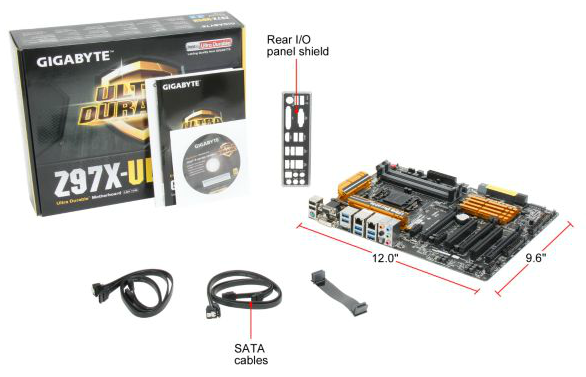
With features like SATA Express and M.2 now taking center stage with the larger motherboards, I wonder if the smaller motherboards with fewer connectors will start to become more worthy recipients for in-the-box additions and out-compete the larger models. However, these additional contents are perhaps apt for the UD5H: with only one USB 3.0 header, there was never going to be a USB 3.0 bracket, and other brackets for COM/USB 2.0 headers are left for EVGA to play with. More SLI bridges are not required – this motherboard (like most Z97) supports only two NVIDIA cards, although they can support three AMD GPUs. At $190, I imagine that some of the other motherboards around this price point will carry WiFi connectivity, which GIGABYTE has redirected that investment into the dual network capabilities.
GIGABYTE Z97X-UD5H Overclocking
Experience with GIGABYTE Z97X-UD5H
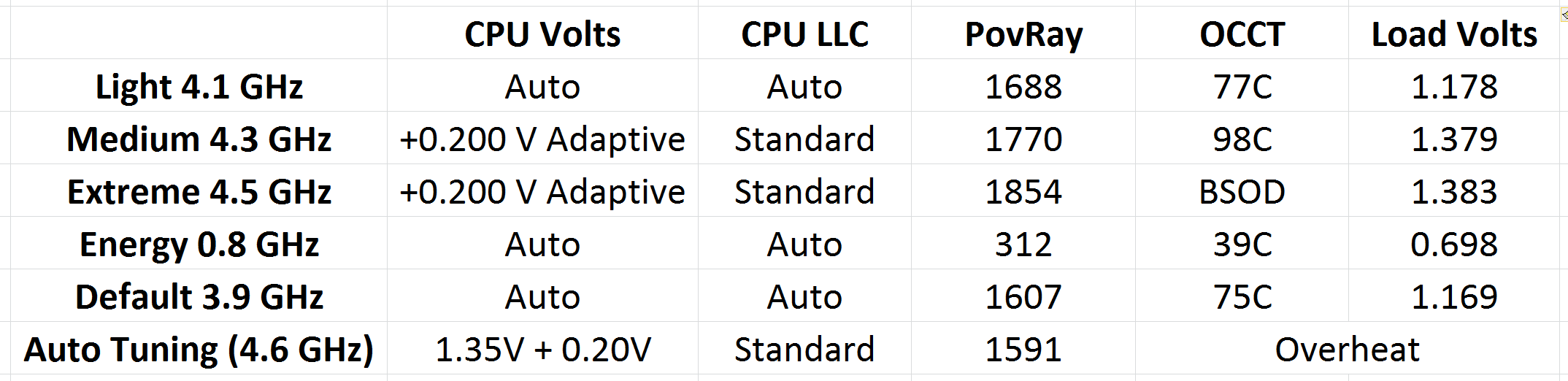
Because we are using our i7-4770K sample from the first Haswell launch, unless motherboard manufacturers have found a trick I was highly doubtful that basic overclocking headroom would change. Haswell processors are characteristically warm, and the temperature becomes the limit before the voltage does on most forms of PC system cooling. The main difference might be at the high end, where extreme overclockers use liquid nitrogen for world records, but GIGABYTE has motherboards for that purpose (such as the Z97X-SOC Force).
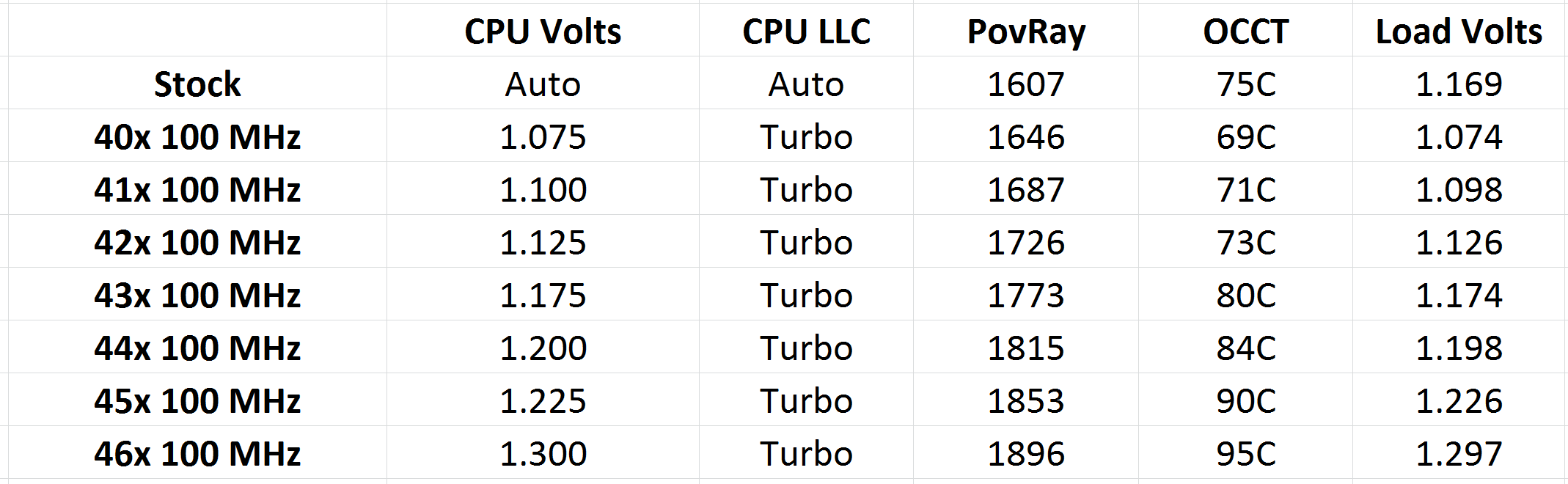
Overclocking on the Z97X-UD5H actually mirrored the experiences with the Z87 counterparts, especially with our sample. Auto-overclocking options used a lot of voltage to ensure compatibility with more CPUs, however some strong cooling is needed for the higher options. Auto tuning was also aggressive, to the point where it failed our stability tests at 4.6 GHz. Manual overclocking gave a 4.6 GHz peak, in line with some of our Z87 motherboards, while reaching a toasty 95C during an OCCT load.
Methodology:
Our standard overclocking methodology is as follows. We select the automatic overclock options and test for stability with PovRay and OCCT to simulate high-end workloads. These stability tests aim to catch any immediate causes for memory or CPU errors.
For manual overclocks, based on the information gathered from previous testing, starts off at a nominal voltage and CPU multiplier, and the multiplier is increased until the stability tests are failed. The CPU voltage is increased gradually until the stability tests are passed, and the process repeated until the motherboard reduces the multiplier automatically (due to safety protocol) or the CPU temperature reaches a stupidly high level (100ºC+). Our test bed is not in a case, which should push overclocks higher with fresher (cooler) air.
Automatic Overclock:
Manual Overclock:


53 Comments
View All Comments
The_Assimilator - Thursday, May 15, 2014 - link
A: By that argument every chipset ever made should still support ISA.B: The Flex IO diagram on this very page specifically states "Total of 14 USB2 ports". I'm reading that as being a constant entirely independent of the number of USB 3.0 ports, but if you have any literature to contradict that, I'd be appreciative if you could link it.
repoman27 - Thursday, May 15, 2014 - link
Not sure I follow your logic. USB is probably the most used feature of a modern chipset (I suppose SATA probably gives it a run for its money though). Take a look at any USB 3.0 connector and you'll find 5 contacts which correspond to the SuperSpeed transmit and receive signaling pairs and ground, and then 4 more that carry the USB 2.0 signal and Vbus. This is how USB 3.0 achieves SuperSpeed while maintaining backwards compatibility, and the signals all need to come from somewhere.Intel hasn't posted datasheets for the 9 series chipsets yet, but there really isn't a heck of a lot of difference between them and the 8 series (in fact they're all currently listed in ARK under the "Products (Formerly Lynx Point)" heading). In the 8 series datasheet [ http://www.intel.com/content/dam/www/public/us/en/... ], however, Intel states: "xHCI USB controller provides support for up to 14 USB ports, of which six can be configured as SuperSpeed USB 3.0 ports." Intel also includes this additional note: "Some USB 3.0 motherboard down devices do not require support for USB 2.0 speed and it is possible to route only the SuperSpeed signals, as allowed by the USB 3.0 specification. In this special case, USB 2.0 and USB 3.0 signals will not need to be paired together, thereby allowing support for more than 14 USB connections."
Interestingly, although the PCH package only provides connections for 14 USB 2.0 signals, those signals can come from either the newer xHCI or the two legacy EHCI controllers which are still present on the chip.
DanNeely - Thursday, May 15, 2014 - link
Am I correctly understanding that as saying that by routing the signals separately you could create a USB3 only port that's not back compatible with USB 1/2?repoman27 - Thursday, May 15, 2014 - link
You're not allowed to do that according to the USB 3.0 Specification, but let's say you had an on board card reader that had a SuperSpeed USB interface, then you wouldn't necessarily be required to route a USB 2.0 signal to it as well and could use that signal for something else instead.repoman27 - Thursday, May 15, 2014 - link
If all the high speed signaling ports were Flex I/O ports, everyone who purchased a PC or motherboard based on that platform would be paying for an insanely large PCIe 2.0 switch with 18 downstream lanes/ports, an 18-port xHCI, and an 18-port SATA 6Gb/s controller plus 18 separate muxes to steer the desired signals to each port. I'm sure Intel would be happy to sell all that to the OEMs instead of just letting them use discrete controllers, but I seriously doubt it would end up lowering the BOM cost any. Flex I/O is just a way to keep the PCH package size down by steering features to a reduced number of balls. I'd rather be able to actually utilize all of the controllers I'm paying for.Not all of the chipsets offer 14 USB ports, and not all of the available USB ports are necessarily routed to external connectors or headers on the logic board. Some of them are used to connect devices on the motherboard itself or other embedded features. Also, since this many ports have been available since the 5 Series, Intel can't exactly regress the feature set while AMD is still offering 14 USB ports.
KAlmquist - Thursday, May 15, 2014 - link
With the current "Flex IO" design, Intel implemented 20 high speed controllers (8 PCIe, 6 SATA, and 6 USB 3.0), but only provided pinouts for 18 of them, meaning that two controllers sit unused. To provide full I/O flexibility, Intel would have to implement 54 controllers (18 of each type), 36 of which would be unused. It sounds like a waste of silicon to me.gloinsir - Wednesday, May 14, 2014 - link
The Rear IO abuses a Renesas USB 3.0 hub to one USB 3.0 port into four, bringing the total number of USB 3.0 ports the motherboard can handle to eight.Oh the poor Renasus abuse.
celestialgrave - Wednesday, May 14, 2014 - link
I guess I don't really see the need for wifi built into my desktop motherboard. I'd rather have the dual NICs. But I guess I can see the advantage when it comes to building a computer for mom or grandma.Ian Cutress - Wednesday, May 14, 2014 - link
If you have a family, more often than not there is a central WiFi router in the house connecting to everyone. If the house/flat isn't all layed out in RJ-45, then if everyone has a computer it has to get the WiFi signal for connections. For example, I have my NAS connected via ethernet to the router, but the three systems in my office are all connected via WiFi, as well as the HTPC in the front room.plopke - Wednesday, May 14, 2014 - link
I am still confused about what PCI-Express and M.2 supposed to be in the end for like a regular consumer? One time i read M.2 stuff and pice express will use the same protocl then other times i read articles like this that they wont work together , etcAny change anyone has some googlde docs spreadsheet that show a table like
connecter type motherboard | protocol | protocol max speed | connecter type SSD | speed SSD | max theorictal performance | compatible