Intel Iris Pro 5200 Graphics Review: Core i7-4950HQ Tested
by Anand Lal Shimpi on June 1, 2013 10:01 AM ESTThe Core i7-4950HQ Mobile CRB
At a high level, Iris Pro 5200 would seem to solve both problems that plagued Intel graphics in the past: a lack of GPU hardware and a lack of memory bandwidth. As a mostly mobile-focused design, and one whose launch partner isn’t keen on giving out early samples, it seemed almost impossible to evaluate Iris Pro in time for the Haswell launch. That was until a week ago when this showed up:
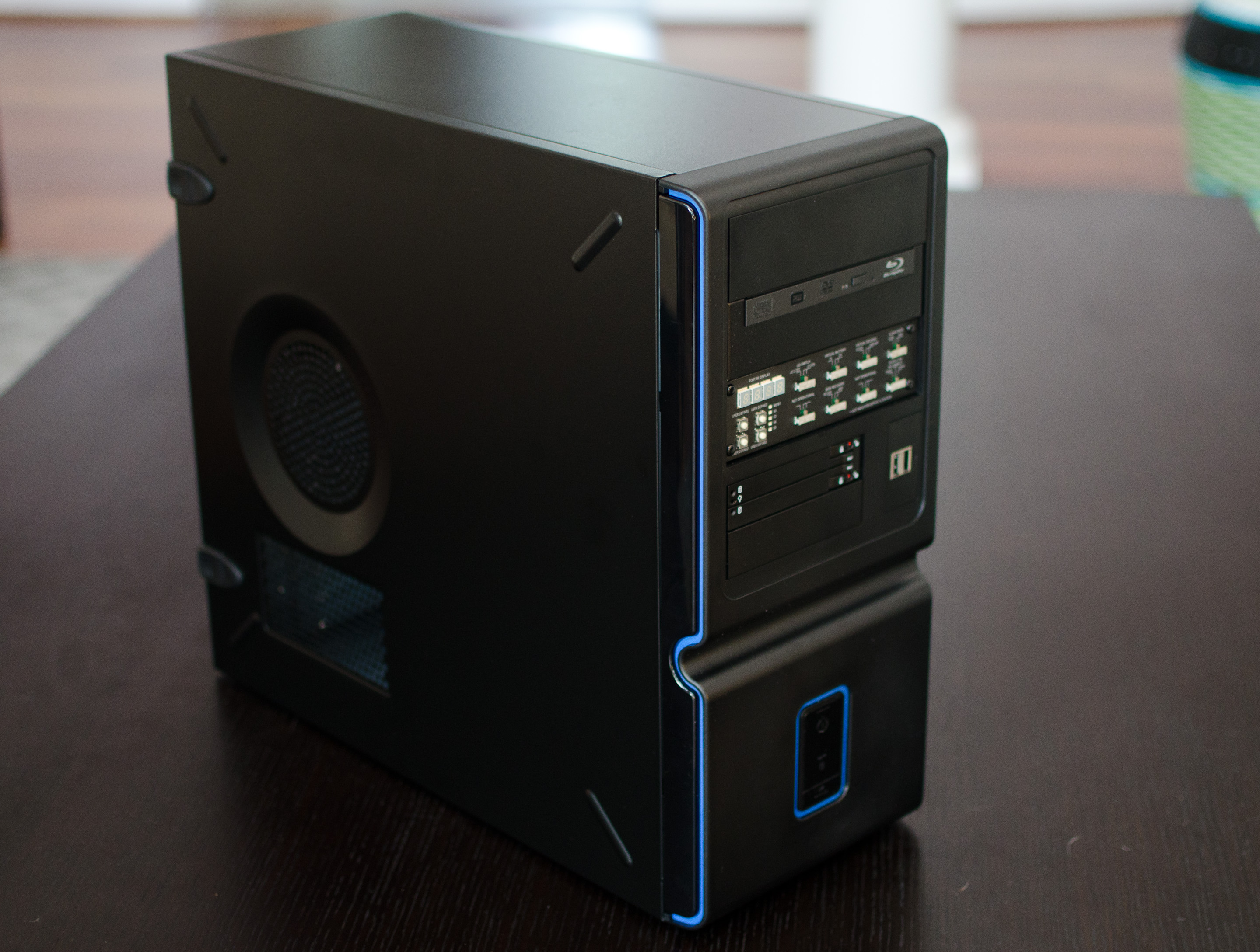
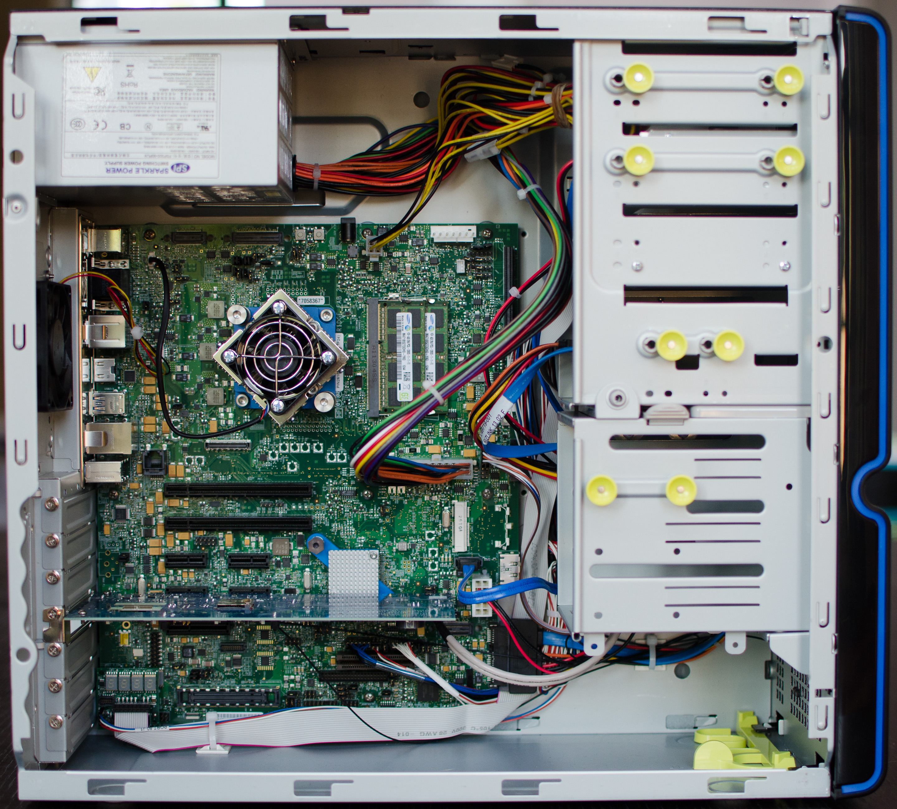
What may look like a funny mid-tower from a few years ago is actually home to one of Intel’s mobile Customer Reference Boards (CRB). Although the chassis is desktop-sized, everything inside is optimized for mobile. It’s just easier to build things larger, especially when it comes to testing and diagnosing problems.
The silicon on-board is a 47W Core i7-4950HQ, the lowest end launch SKU with Iris Pro 5200 graphics. The chassis is obviously overkill for a 47W part, but the performance we get with this machine should be representative of any i7-4950HQ system with a cooler capable of dissipating 47W.
If you read our Haswell CPU review you’ll know that Intel tried to be stingy with telling us die sizes and transistor counts for the bulk of the Haswell lineup, electing to only give us data on dual-core Haswell GT3 and quad-core Haswell GT2. Knowing that mobile parts ship without integrated heat spreaders, I went to work on pulling off the i7-4950HQ’s heatsink (after I finished testing, just in case).
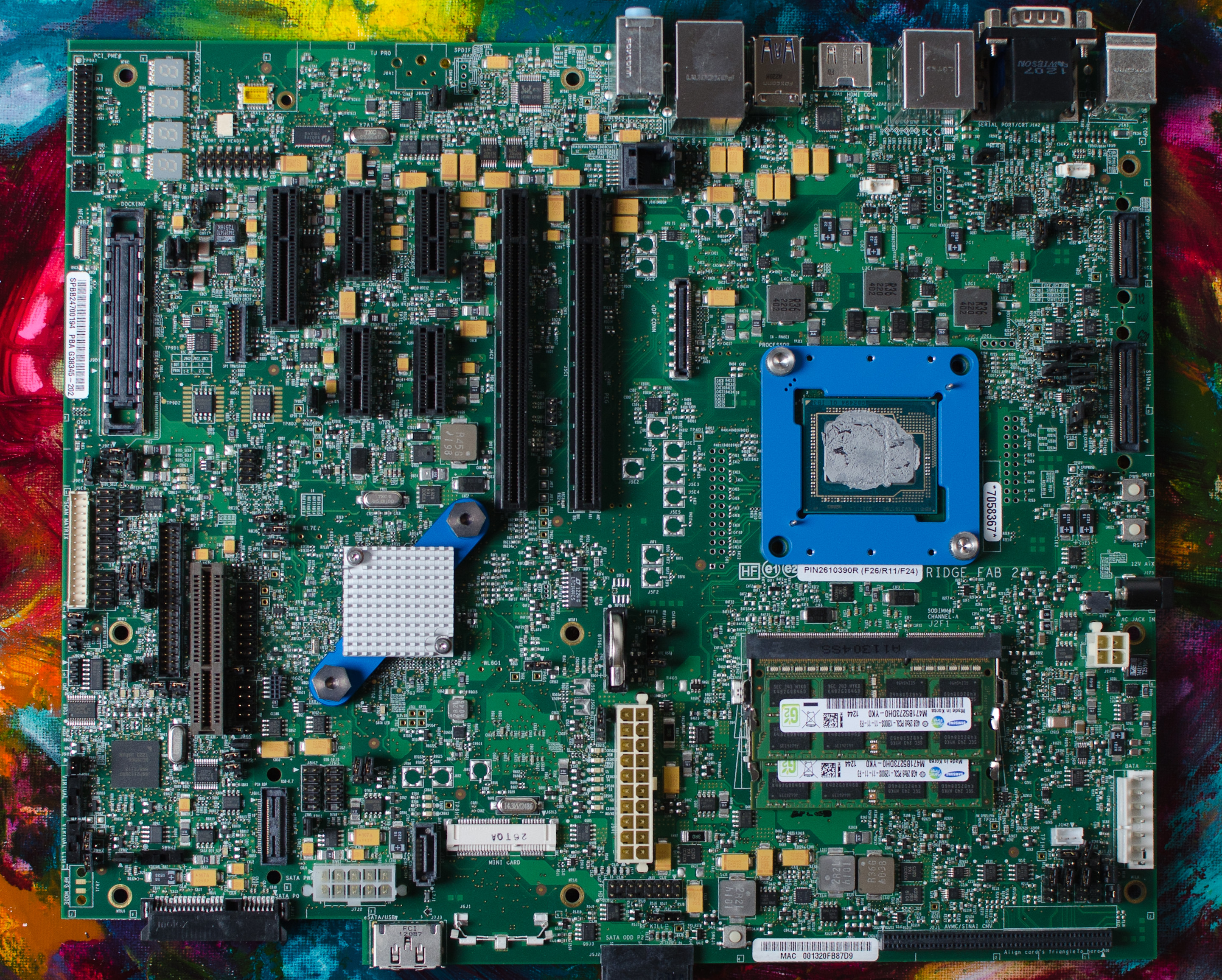
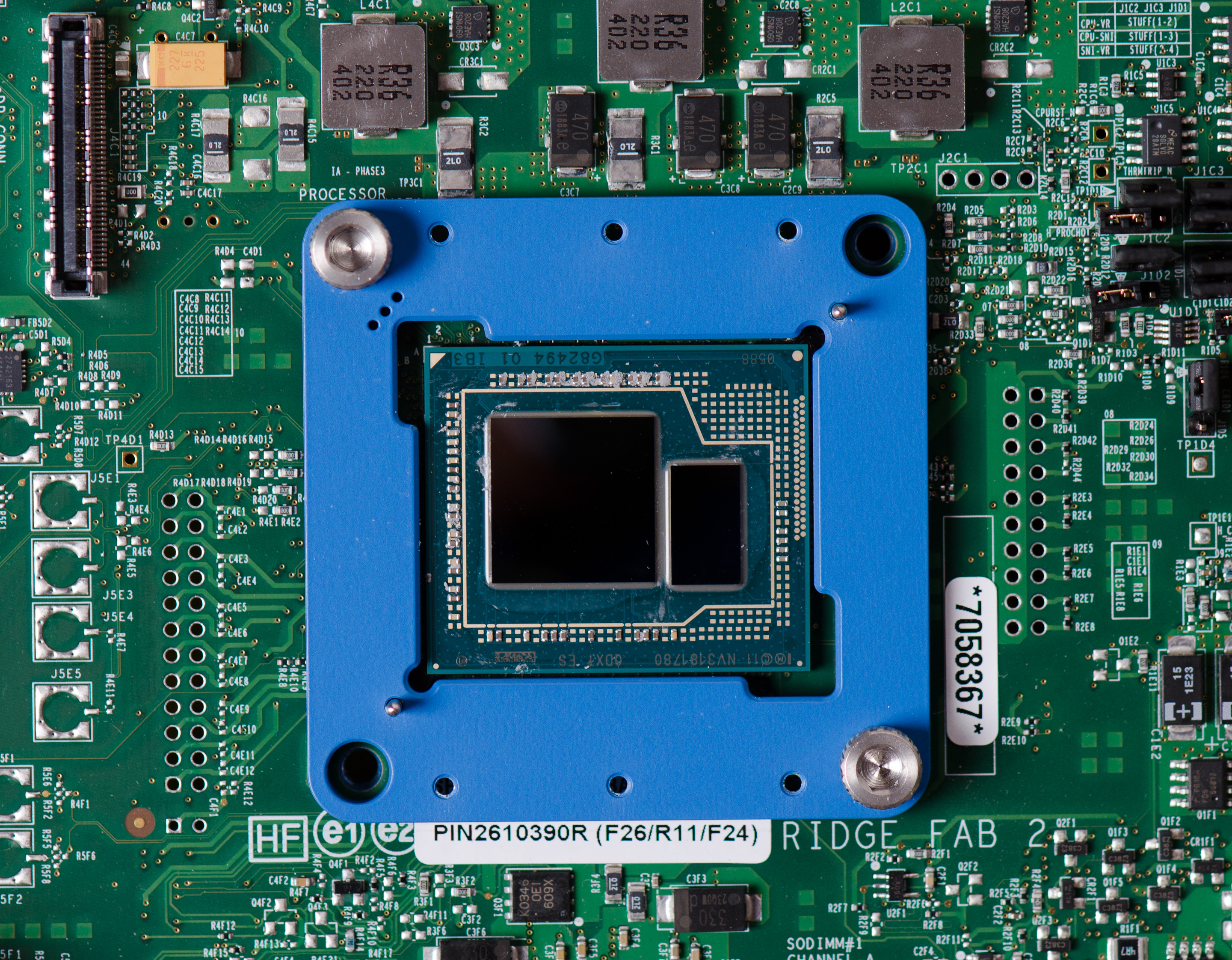
With the heatsink off and thermal paste wiped off, I used my bargain basement calipers to get a rough idea of die area. This is what I came up with:
| Intel Haswell | |||||||||||||||||
| CPU Configuration | GPU Configuration | Die Size | Transistor Count | ||||||||||||||
| Haswell GT3e (QC) | Quad-Core | GT3e | 264mm2 + 84mm2 | ? | |||||||||||||
| Haswell GT2 (QC) | Quad-Core | GT2 | 177mm2 | 1.4B | |||||||||||||
| Haswell ULT GT3 | Dual-Core | GT3 | 181mm2 | 1.3B | |||||||||||||
The Crystalwell die measures 7mm x 12mm (84mm^2), while the quad-core Haswell + GT3 die is a whopping 264mm^2 (16.2mm x 16.3mm). Working backwards from the official data Intel provided (177mm^2 for quad-core GT2), I came up with an 87mm^2 adder for the extra hardware in Haswell GT3 vs. GT2. Doubling that 87mm^2 we get a rough idea of how big the full 40 EU Haswell GPU might be: 174mm^2. If my math is right, this means that in a quad-core Haswell GT3 die, around 65% of the die area is GPU. This is contrary to the ~33% in a quad-core Haswell GT2. I suspect a dual-core + GT3 design is at least half GPU.


177 Comments
View All Comments
arjunp2085 - Sunday, June 2, 2013 - link
I was under the impression that Richland has been selling on newegg as per a comment on an earlier article..I was also wondering since you had done a review on Richland from MSI notebook review i was wondering if you would do a similar comparison..
http://www.anandtech.com/show/6949/msi-gx70-3be-ri...
It would be appreciated just placing all the possible matches on the table and a paragraph with selection criteria for the review making the choices dispelling opinion of missing any models
GameHopper - Sunday, June 2, 2013 - link
Why no real power measurements? If it's so important to iris Pro, real world power numbers will be more useful than just listing TDP of the partsshinkueagle - Sunday, June 2, 2013 - link
The GIANT has awoken! Performance-wise, its amazing! Destroys Trinity! Price-wise.... Well, the area needs some work...trip1ex - Sunday, June 2, 2013 - link
Yes really disappointed there is no socketed cpu solution that have the best igpu config.But I suppose I already have Ivy Bridge i5 for my WMC pc and it is good enough. Still be a nice cheap way to build a secondary small desktop that could also do some light gaming.
Lataa - Sunday, June 2, 2013 - link
dikicha23@gmail.comvFunct - Sunday, June 2, 2013 - link
Curious why Intel just doesn't go straight for the jugular and release a discrete GPU part on their 22nm process. NVidia/AMD is stuck at 28mm because of their foundries, and it appears Intel's GPU architecture is feature complete and therefore competitive with the discrete parts if they scaled up everything by 4x or 5x.NVidia & AMD should be worried about their core high-profit-margins business!
jamescox - Sunday, June 2, 2013 - link
The photo you have on page 4 showing the 2 separate die is strange. The haswell die should not be square. Other photos I have seen show the expected (extremely rectangular) haswell die and a tiny ram chip. I would expect a haswell based chip with double the cpu (8 real cores), and no gpu eventually; this would be almost square. Do you know why your chip does not match other multi-chip module photos online?jamescox - Tuesday, June 4, 2013 - link
I guess the other photos are haswell plus an integrated chipset in the same module. The photo of the two die is still strange, as neither of these look like a haswell die.IntelUser2000 - Tuesday, June 4, 2013 - link
That's because that's the picture for GT3e Iris Pro 5200 graphics. The bigger square die is the Haswell CPU+GT3 GPU, while the smaller one is the on-package DRAM.The dual core with on-package chipset is even longer than the regular Haswell.
tipoo - Wednesday, January 21, 2015 - link
Yes it should, you're thinking of the ultrabook chips with a controller to the side, not eDRAM. Those ones are rectangular. Look at a haswell MBP 15" teardown to verify.