Intel Iris Pro 5200 Graphics Review: Core i7-4950HQ Tested
by Anand Lal Shimpi on June 1, 2013 10:01 AM ESTThe Core i7-4950HQ Mobile CRB
At a high level, Iris Pro 5200 would seem to solve both problems that plagued Intel graphics in the past: a lack of GPU hardware and a lack of memory bandwidth. As a mostly mobile-focused design, and one whose launch partner isn’t keen on giving out early samples, it seemed almost impossible to evaluate Iris Pro in time for the Haswell launch. That was until a week ago when this showed up:
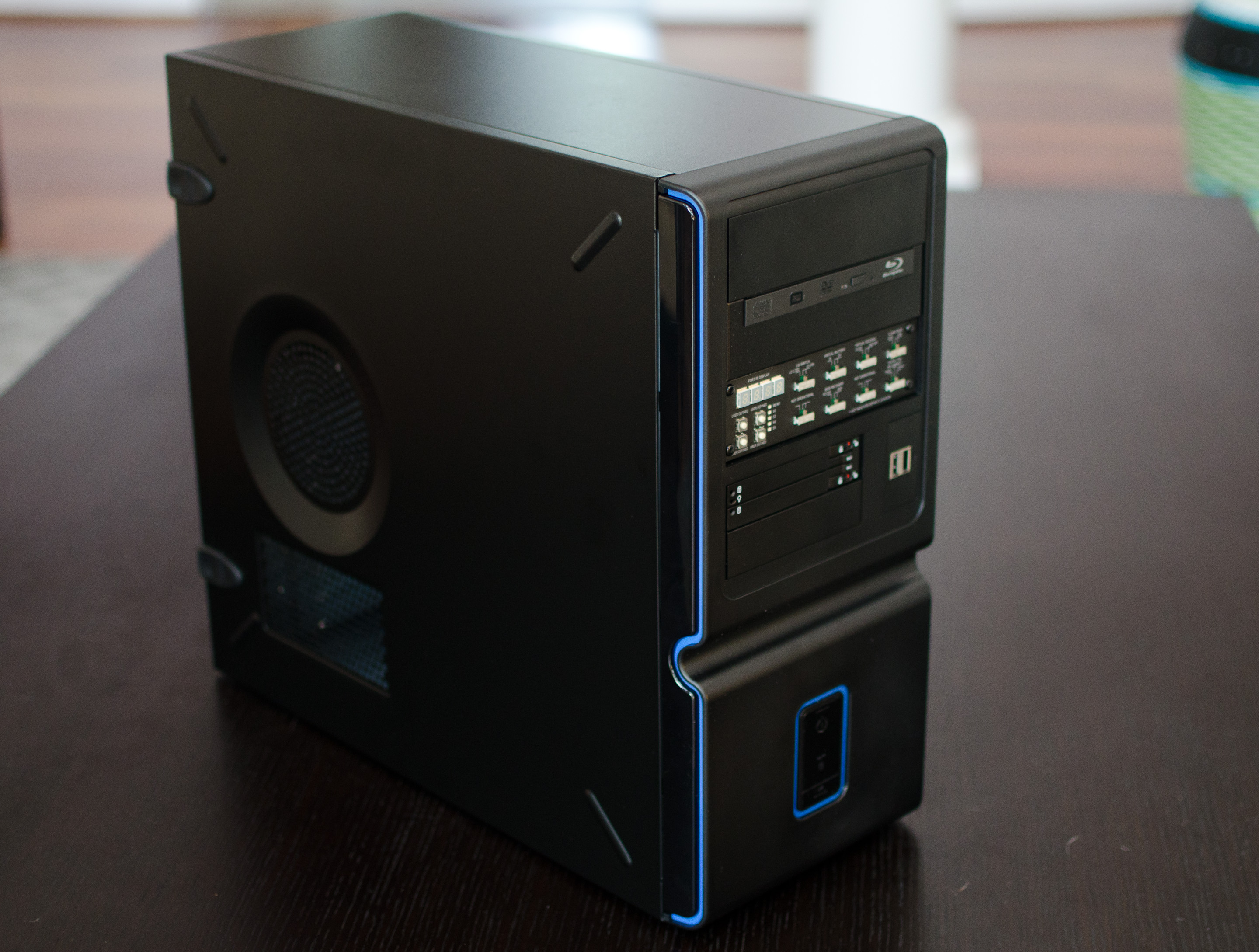
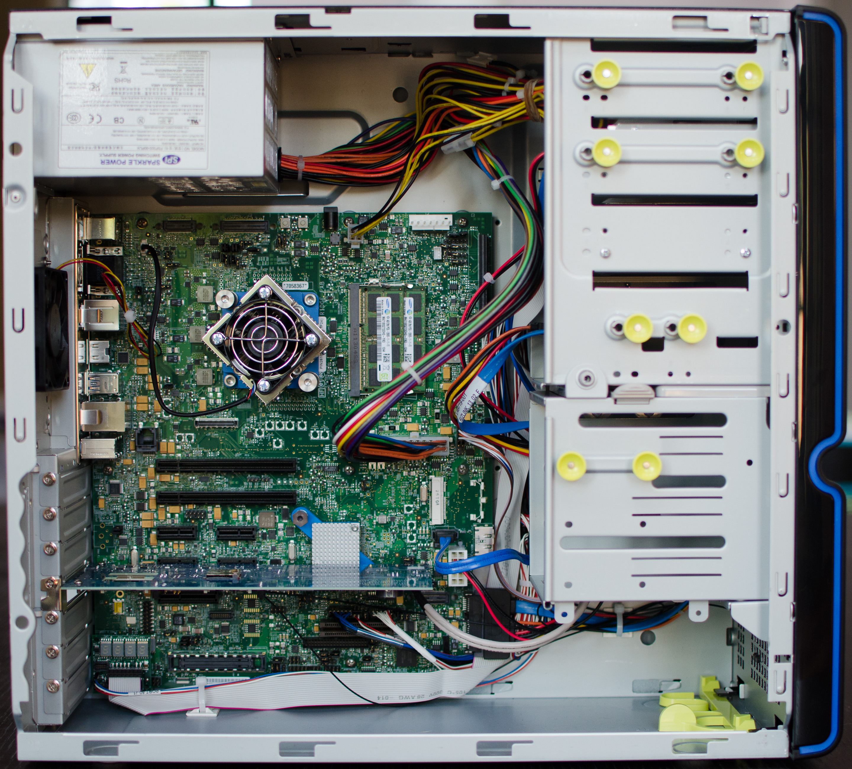
What may look like a funny mid-tower from a few years ago is actually home to one of Intel’s mobile Customer Reference Boards (CRB). Although the chassis is desktop-sized, everything inside is optimized for mobile. It’s just easier to build things larger, especially when it comes to testing and diagnosing problems.
The silicon on-board is a 47W Core i7-4950HQ, the lowest end launch SKU with Iris Pro 5200 graphics. The chassis is obviously overkill for a 47W part, but the performance we get with this machine should be representative of any i7-4950HQ system with a cooler capable of dissipating 47W.
If you read our Haswell CPU review you’ll know that Intel tried to be stingy with telling us die sizes and transistor counts for the bulk of the Haswell lineup, electing to only give us data on dual-core Haswell GT3 and quad-core Haswell GT2. Knowing that mobile parts ship without integrated heat spreaders, I went to work on pulling off the i7-4950HQ’s heatsink (after I finished testing, just in case).
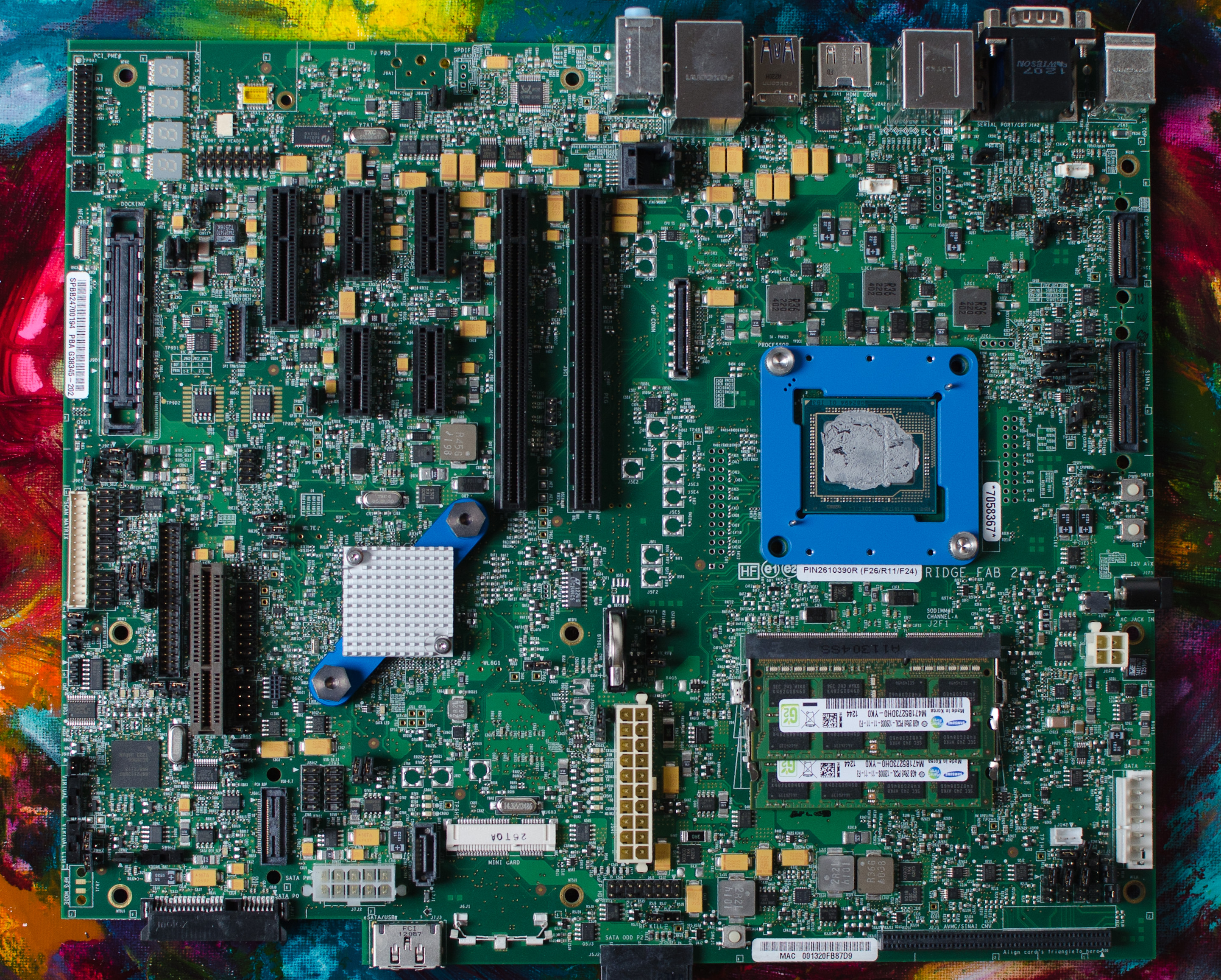
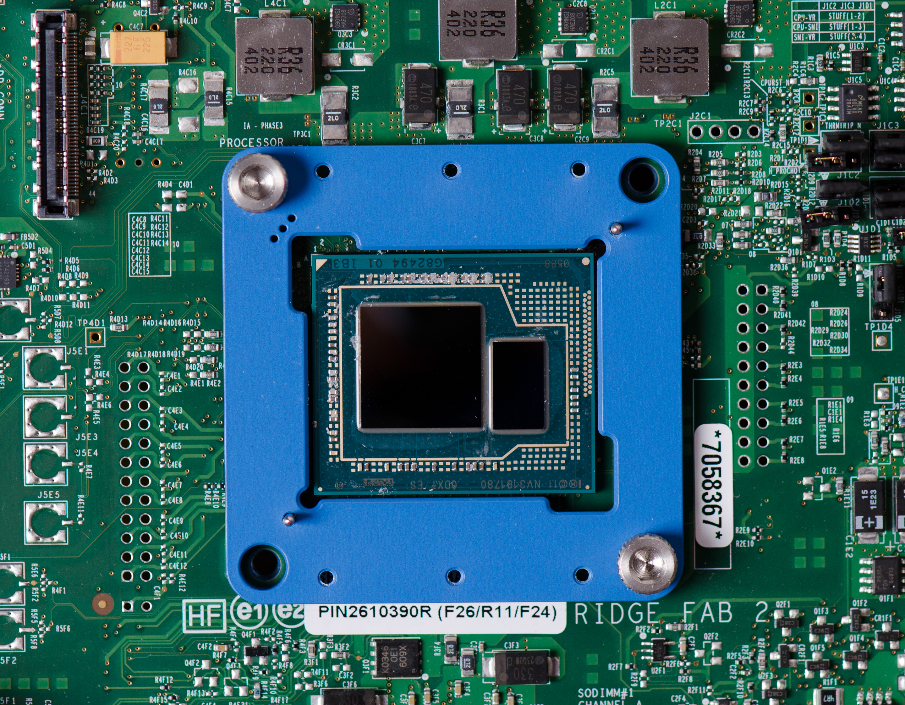
With the heatsink off and thermal paste wiped off, I used my bargain basement calipers to get a rough idea of die area. This is what I came up with:
| Intel Haswell | |||||||||||||||||
| CPU Configuration | GPU Configuration | Die Size | Transistor Count | ||||||||||||||
| Haswell GT3e (QC) | Quad-Core | GT3e | 264mm2 + 84mm2 | ? | |||||||||||||
| Haswell GT2 (QC) | Quad-Core | GT2 | 177mm2 | 1.4B | |||||||||||||
| Haswell ULT GT3 | Dual-Core | GT3 | 181mm2 | 1.3B | |||||||||||||
The Crystalwell die measures 7mm x 12mm (84mm^2), while the quad-core Haswell + GT3 die is a whopping 264mm^2 (16.2mm x 16.3mm). Working backwards from the official data Intel provided (177mm^2 for quad-core GT2), I came up with an 87mm^2 adder for the extra hardware in Haswell GT3 vs. GT2. Doubling that 87mm^2 we get a rough idea of how big the full 40 EU Haswell GPU might be: 174mm^2. If my math is right, this means that in a quad-core Haswell GT3 die, around 65% of the die area is GPU. This is contrary to the ~33% in a quad-core Haswell GT2. I suspect a dual-core + GT3 design is at least half GPU.


177 Comments
View All Comments
8steve8 - Saturday, June 1, 2013 - link
Great work intel, and great review anand.As a fan of low power and small form factor high performance pcs, I'm excited about the 4770R.
my question is how do we get a system with 4770R ?
will it be in an NUC, if so, when/info?
will there be mini-itx motherboards with it soldered on?
bill5 - Saturday, June 1, 2013 - link
Anand, would you say the lack of major performance improvement due to crystalwell bodes ill for Xbox one?The idea is ESRAM could make the 1.2 TF Xbox One GPU "punch above it's weight" with more efficiency due to the 32MB of low latency cache (ALU's will stall less waiting on data). However these results dont really show that for Haswell (the compute results that scale perfectly with ALU's for example).
Here note I'm distinguishing between the cache as bandwidth saver, I think we can all agree it will serve that purpose- and as actual performance enhancer. I'm interested in the latter for Xbox One.
Kevin G - Saturday, June 1, 2013 - link
A couple of quotes and comments from the article:"If Crystalwell demand is lower than expected, Intel still has a lot of quad-core GT3 Haswell die that it can sell and vice versa."
Intel is handicapping demand for GT3e parts by not shipping them in socketed form. I'd love to upgrade my i7-2600k system to a 4770K+GT3e+TSX setup. Seriously Intel, ship that part and take my money.
"The Crystalwell enabled graphics driver can choose to keep certain things out of the eDRAM. The frame buffer isn’t stored in eDRAM for example."
WTF?!? The eDRAM would be the ideal place to store various frequently used buffers. Having 128 MB of memory leaves plenty of room for streaming in textures as need be. The only reason not to hold the full frame buffer is if Intel has an aggressive tile based rendering design and only a tile is stored there. I suspect that Intel's driver team will change this in the future.
"An Ultrabook SKU with Crystalwell would make a ton of sense, but given where Ultrabooks are headed (price-wise) I’m not sure Intel could get any takers."
I bet Apple would ship a GT3e based part in the MacBook Air form factor. They'd do something like lower the GPU clocks to prevent it from melting but they want it. It wouldn't surprise me if Apple managed to negotiate a custom part from Intel again.
Ultimatley I'm pleased with GT3e. On the desktop I can see the GPU being used for OpenCL tasks like physics while my Radeon 7970 handles the rest of the graphics load. Or for anything else, I'd like GT3e for the massive L4 cache.
tipoo - Saturday, June 1, 2013 - link
"Ultimatley I'm pleased with GT3e. On the desktop I can see the GPU being used for OpenCL tasks like physics while my Radeon 7970 handles the rest of the graphics load. Or for anything else, I'd like GT3e for the massive L4 cache."I'd love that to work, but what developer would include that functionality for that niche setup?
Kevin G - Saturday, June 1, 2013 - link
OpenCL is supposed to be flexible enough that you can mix execution targets. This also includes the possibility of OpenCL drivers for CPU's in addition to those that use GPU's. At the very least, it'd be nice for a game or application to manually select the OpenCL target in some config file.Egg - Saturday, June 1, 2013 - link
I'm only a noob high school junior, but aren't frame buffers tossed after display? What would be the point of storing a frame buffer? You don't reuse the data in it at all. As far as I know, frame buffer != unpacked textures.Also, aren't most modern fully programmable GPUs not tile based at all?
Also, wasn't it mentioned that K-series parts don't have TSX?
Kevin G - Saturday, June 1, 2013 - link
The z-buffer in particular is written and often read. Deferred rendering also blends multiple buffers together and at 128 MB in size, a deferred render can keep several in that memory. AA algorithms also perform read/writes on the buffer. At some point, I do see Intel moving the various buffers into the 128 MB of eDRAM as drivers mature. In fairness, this change may not be universal to all games and dependent on things like resolution.Then again, it could be a true cache for the GPU. This would mean that the drivers do not explicitly store the frame buffers there but can could be stored there based upon prefetching of data. Intel's caching hierarchy is a bit weird as the CPU's L3 cache can also be used as a L4 cache for the GPU under HD2000/2500/3000/4000 parts. Presumably the eDRAM would be a L5 cache under the Sandy Bridge/Ivy Bridge schema. The eDRAM has been described as a victim cache though for GPU operations it would make sense to prefetch large amounts of data (textures, buffers). It'd be nice to get some clarification on this with Haswell.
PowerVR is still tile based. Previous Intel integrated solutions were also tile base though they dropped that with the HD line (and I can't remember if the GMA line was tile based as well).
And you are correct that the K series don't have TSX, hence why I'd like a 4770K with GT3e and TSX. Also I forgot to throw in VT-d since that too is arbitrarily disabled in the K series.
IntelUser2000 - Sunday, June 2, 2013 - link
Kevin G: Intel dropped the Tile-based rendering in the GMA 3 series generation back in 2006. Although, their Tile rendering was different from PowerVR's.Egg - Sunday, June 2, 2013 - link
Fair points - I was being a bit myopic and only thought about buffers persisting across frames, neglecting the fact that buffers often need to be reused within the process of rendering a single frame! Can you explain how the CPU's L3 cache is an L4 cache for the GPU? Does the GPU have its own L3 cache already?Also I don't know whether PowerVR's architecture is considered fully programmable yet. I know they have OpenCL capabilities, but reading http://www.anandtech.com/show/6112/qualcomms-quadc... I'm getting a vague feeling that it isn't as complete as GCN or Kepler, feature wise.
IntelUser2000 - Tuesday, June 4, 2013 - link
Gen 7, the Ivy Bridge generation, has its own L3 cache. So you have the LLC(which is L3 for the CPU), and its own L3. Haswell is Gen 7.5.