Intel Iris Pro 5200 Graphics Review: Core i7-4950HQ Tested
by Anand Lal Shimpi on June 1, 2013 10:01 AM EST
The Prelude
As Intel got into the chipset business it quickly found itself faced with an interesting problem. As the number of supported IO interfaces increased (back then we were talking about things like AGP, FSB), the size of the North Bridge die had to increase in order to accommodate all of the external facing IO. Eventually Intel ended up in a situation where IO dictated a minimum die area for the chipset, but the actual controllers driving that IO didn’t need all of that die area. Intel effectively had some free space on its North Bridge die to do whatever it wanted with. In the late 90s Micron saw this problem and contemplating throwing some L3 cache onto its North Bridges. Intel’s solution was to give graphics away for free.
The budget for Intel graphics was always whatever free space remained once all other necessary controllers in the North Bridge were accounted for. As a result, Intel’s integrated graphics was never particularly good. Intel didn’t care about graphics, it just had some free space on a necessary piece of silicon and decided to do something with it. High performance GPUs need lots of transistors, something Intel would never give its graphics architects - they only got the bare minimum. It also didn’t make sense to focus on things like driver optimizations and image quality. Investing in people and infrastructure to support something you’re giving away for free never made a lot of sense.
Intel hired some very passionate graphics engineers, who always petitioned Intel management to give them more die area to work with, but the answer always came back no. Intel was a pure blooded CPU company, and the GPU industry wasn’t interesting enough at the time. Intel’s GPU leadership needed another approach.
A few years ago they got that break. Once again, it had to do with IO demands on chipset die area. Intel’s chipsets were always built on a n-1 or n-2 process. If Intel was building a 45nm CPU, the chipset would be built on 65nm or 90nm. This waterfall effect allowed Intel to help get more mileage out of its older fabs, which made the accountants at Intel quite happy as those $2 - $3B buildings are painfully useless once obsolete. As the PC industry grew, so did shipments of Intel chipsets. Each Intel CPU sold needed at least one other Intel chip built on a previous generation node. Interface widths as well as the number of IOs required on chipsets continued to increase, driving chipset die areas up once again. This time however, the problem wasn’t as easy to deal with as giving the graphics guys more die area to work with. Looking at demand for Intel chipsets, and the increasing die area, it became clear that one of two things had to happen: Intel would either have to build more fabs on older process nodes to keep up with demand, or Intel would have to integrate parts of the chipset into the CPU.
Not wanting to invest in older fab technology, Intel management green-lit the second option: to move the Graphics and Memory Controller Hub onto the CPU die. All that would remain off-die would be a lightweight IO controller for things like SATA and USB. PCIe, the memory controller, and graphics would all move onto the CPU package, and then eventually share the same die with the CPU cores.
Pure economics and an unwillingness to invest in older fabs made the GPU a first class citizen in Intel silicon terms, but Intel management still didn’t have the motivation to dedicate more die area to the GPU. That encouragement would come externally, from Apple.
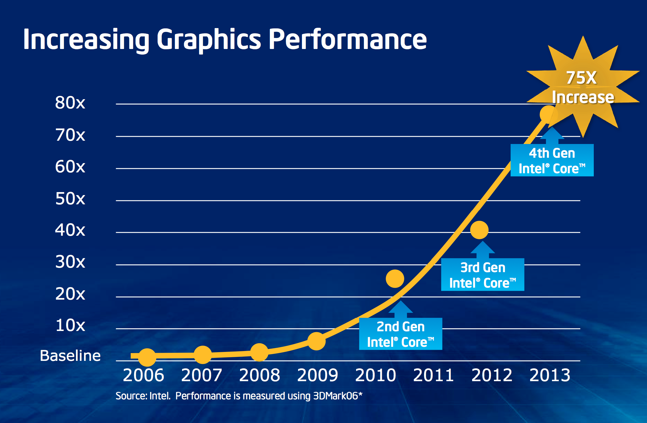
Looking at the past few years of Apple products, you’ll recognize one common thread: Apple as a company values GPU performance. As a small customer of Intel’s, Apple’s GPU desires didn’t really matter, but as Apple grew, so did its influence within Intel. With every microprocessor generation, Intel talks to its major customers and uses their input to help shape the designs. There’s no sense in building silicon that no one wants to buy, so Intel engages its customers and rolls their feedback into silicon. Apple eventually got to the point where it was buying enough high-margin Intel silicon to influence Intel’s roadmap. That’s how we got Intel’s HD 3000. And that’s how we got here.


177 Comments
View All Comments
8steve8 - Saturday, June 1, 2013 - link
Great work intel, and great review anand.As a fan of low power and small form factor high performance pcs, I'm excited about the 4770R.
my question is how do we get a system with 4770R ?
will it be in an NUC, if so, when/info?
will there be mini-itx motherboards with it soldered on?
bill5 - Saturday, June 1, 2013 - link
Anand, would you say the lack of major performance improvement due to crystalwell bodes ill for Xbox one?The idea is ESRAM could make the 1.2 TF Xbox One GPU "punch above it's weight" with more efficiency due to the 32MB of low latency cache (ALU's will stall less waiting on data). However these results dont really show that for Haswell (the compute results that scale perfectly with ALU's for example).
Here note I'm distinguishing between the cache as bandwidth saver, I think we can all agree it will serve that purpose- and as actual performance enhancer. I'm interested in the latter for Xbox One.
Kevin G - Saturday, June 1, 2013 - link
A couple of quotes and comments from the article:"If Crystalwell demand is lower than expected, Intel still has a lot of quad-core GT3 Haswell die that it can sell and vice versa."
Intel is handicapping demand for GT3e parts by not shipping them in socketed form. I'd love to upgrade my i7-2600k system to a 4770K+GT3e+TSX setup. Seriously Intel, ship that part and take my money.
"The Crystalwell enabled graphics driver can choose to keep certain things out of the eDRAM. The frame buffer isn’t stored in eDRAM for example."
WTF?!? The eDRAM would be the ideal place to store various frequently used buffers. Having 128 MB of memory leaves plenty of room for streaming in textures as need be. The only reason not to hold the full frame buffer is if Intel has an aggressive tile based rendering design and only a tile is stored there. I suspect that Intel's driver team will change this in the future.
"An Ultrabook SKU with Crystalwell would make a ton of sense, but given where Ultrabooks are headed (price-wise) I’m not sure Intel could get any takers."
I bet Apple would ship a GT3e based part in the MacBook Air form factor. They'd do something like lower the GPU clocks to prevent it from melting but they want it. It wouldn't surprise me if Apple managed to negotiate a custom part from Intel again.
Ultimatley I'm pleased with GT3e. On the desktop I can see the GPU being used for OpenCL tasks like physics while my Radeon 7970 handles the rest of the graphics load. Or for anything else, I'd like GT3e for the massive L4 cache.
tipoo - Saturday, June 1, 2013 - link
"Ultimatley I'm pleased with GT3e. On the desktop I can see the GPU being used for OpenCL tasks like physics while my Radeon 7970 handles the rest of the graphics load. Or for anything else, I'd like GT3e for the massive L4 cache."I'd love that to work, but what developer would include that functionality for that niche setup?
Kevin G - Saturday, June 1, 2013 - link
OpenCL is supposed to be flexible enough that you can mix execution targets. This also includes the possibility of OpenCL drivers for CPU's in addition to those that use GPU's. At the very least, it'd be nice for a game or application to manually select the OpenCL target in some config file.Egg - Saturday, June 1, 2013 - link
I'm only a noob high school junior, but aren't frame buffers tossed after display? What would be the point of storing a frame buffer? You don't reuse the data in it at all. As far as I know, frame buffer != unpacked textures.Also, aren't most modern fully programmable GPUs not tile based at all?
Also, wasn't it mentioned that K-series parts don't have TSX?
Kevin G - Saturday, June 1, 2013 - link
The z-buffer in particular is written and often read. Deferred rendering also blends multiple buffers together and at 128 MB in size, a deferred render can keep several in that memory. AA algorithms also perform read/writes on the buffer. At some point, I do see Intel moving the various buffers into the 128 MB of eDRAM as drivers mature. In fairness, this change may not be universal to all games and dependent on things like resolution.Then again, it could be a true cache for the GPU. This would mean that the drivers do not explicitly store the frame buffers there but can could be stored there based upon prefetching of data. Intel's caching hierarchy is a bit weird as the CPU's L3 cache can also be used as a L4 cache for the GPU under HD2000/2500/3000/4000 parts. Presumably the eDRAM would be a L5 cache under the Sandy Bridge/Ivy Bridge schema. The eDRAM has been described as a victim cache though for GPU operations it would make sense to prefetch large amounts of data (textures, buffers). It'd be nice to get some clarification on this with Haswell.
PowerVR is still tile based. Previous Intel integrated solutions were also tile base though they dropped that with the HD line (and I can't remember if the GMA line was tile based as well).
And you are correct that the K series don't have TSX, hence why I'd like a 4770K with GT3e and TSX. Also I forgot to throw in VT-d since that too is arbitrarily disabled in the K series.
IntelUser2000 - Sunday, June 2, 2013 - link
Kevin G: Intel dropped the Tile-based rendering in the GMA 3 series generation back in 2006. Although, their Tile rendering was different from PowerVR's.Egg - Sunday, June 2, 2013 - link
Fair points - I was being a bit myopic and only thought about buffers persisting across frames, neglecting the fact that buffers often need to be reused within the process of rendering a single frame! Can you explain how the CPU's L3 cache is an L4 cache for the GPU? Does the GPU have its own L3 cache already?Also I don't know whether PowerVR's architecture is considered fully programmable yet. I know they have OpenCL capabilities, but reading http://www.anandtech.com/show/6112/qualcomms-quadc... I'm getting a vague feeling that it isn't as complete as GCN or Kepler, feature wise.
IntelUser2000 - Tuesday, June 4, 2013 - link
Gen 7, the Ivy Bridge generation, has its own L3 cache. So you have the LLC(which is L3 for the CPU), and its own L3. Haswell is Gen 7.5.