The Apple iPad Review (2012)
by Vivek Gowri & Anand Lal Shimpi on March 28, 2012 3:14 PM ESTA Word on Packaging
Unlike the first two iPads, the 3rd generation iPad abandons the high density flip-chip PoP SoC/DRAM stack and uses a discrete, flip-chip BGA package for the SoC and two discrete BGA packages for the DRAMs.
If you think of SoC silicon as a stack, the lowest layer is where you'll find the actual transistor logic, while the layers of metal above it connect everything together. In the old days, the silicon stack would sit just as I've described it—logic at the bottom, metal layers on top. Pads around the perimeter of the top of the silicon would connect to very thin wires, that would then route to the package substrate and eventually out to balls or pins on the underside of the package. These wire bonded packages, as they were called, had lower limits of how many pins you could have connecting to your chip.
There are also cooling concerns. In a traditional wire bonded package, your cooling solution ultimately rests on a piece of your packaging substrate. The actual silicon itself isn't exposed.
As its name implies, a flip-chip package is literally the inverse of this. Instead of the metal layers being at the top of the stack, before packaging the silicon is inverted and the metal layers are at the bottom of the stack. Solder bumps at the top of the silicon stack (now flipped and at the bottom) connect the topmost metal layer to the package itself. Since we're dealing with solder bumps on the silicon itself rather than wires routed to the edge of the silicon, there's much more surface area for signals to get in/out of the silicon.
Since the chip is flipped, the active logic is now exposed in a flip-chip package and the hottest part of the silicon can be directly attached to a cooling solution.
An example of a PoP stack
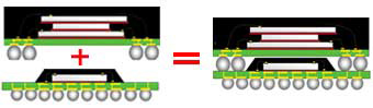
To save on PCB real estate however, many SoC vendors would take a flip-chip SoC and stack DRAM on top of it in a package-on-package (PoP) configuration. Ultimately this re-introduces many of the problems from older packaging techniques—mainly it becomes difficult to have super wide memory interfaces as your ball-out for the PoP stack is limited to the area around your die, and cooling is a concern once more. For low power, low bandwidth mobile SoCs this hasn't really been a problem, which is why we see PoP stacks deployed all over the place.
Take a look at the A5, a traditional FC-BGA SoC with PoP DRAM vs. the A5X (this isn't to scale):
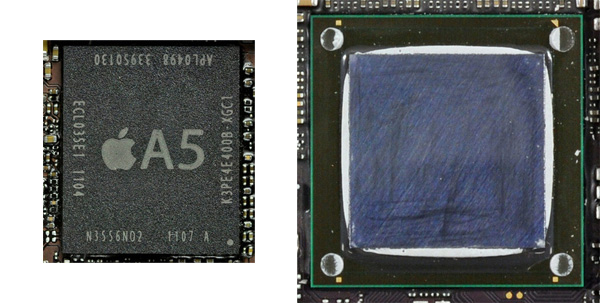
Images courtesy iFixit
The A5X in this case is a FC-BGA SoC but without any DRAM stacked on top of it. The A5X is instead covered in a thermally conductive paste and then with a metallic heatspreader to conduct heat away from the SoC and protect the silicon.
Given the size and complexity of the A5X SoC, it's no surprise that Apple didn't want to insulate the silicon with a stack of DRAM on top of it. In typical package-on-package stacks, you'd see solder bumps around the silicon, on the package itself, that a separate DRAM package would adhere to. Instead of building up a PoP stack here, Apple simply located its two 64-bit DRAM devices on the opposite side of the iPad's logic board and routed the four 32-bit LP-DDR2 memory channels through the PCB layers.
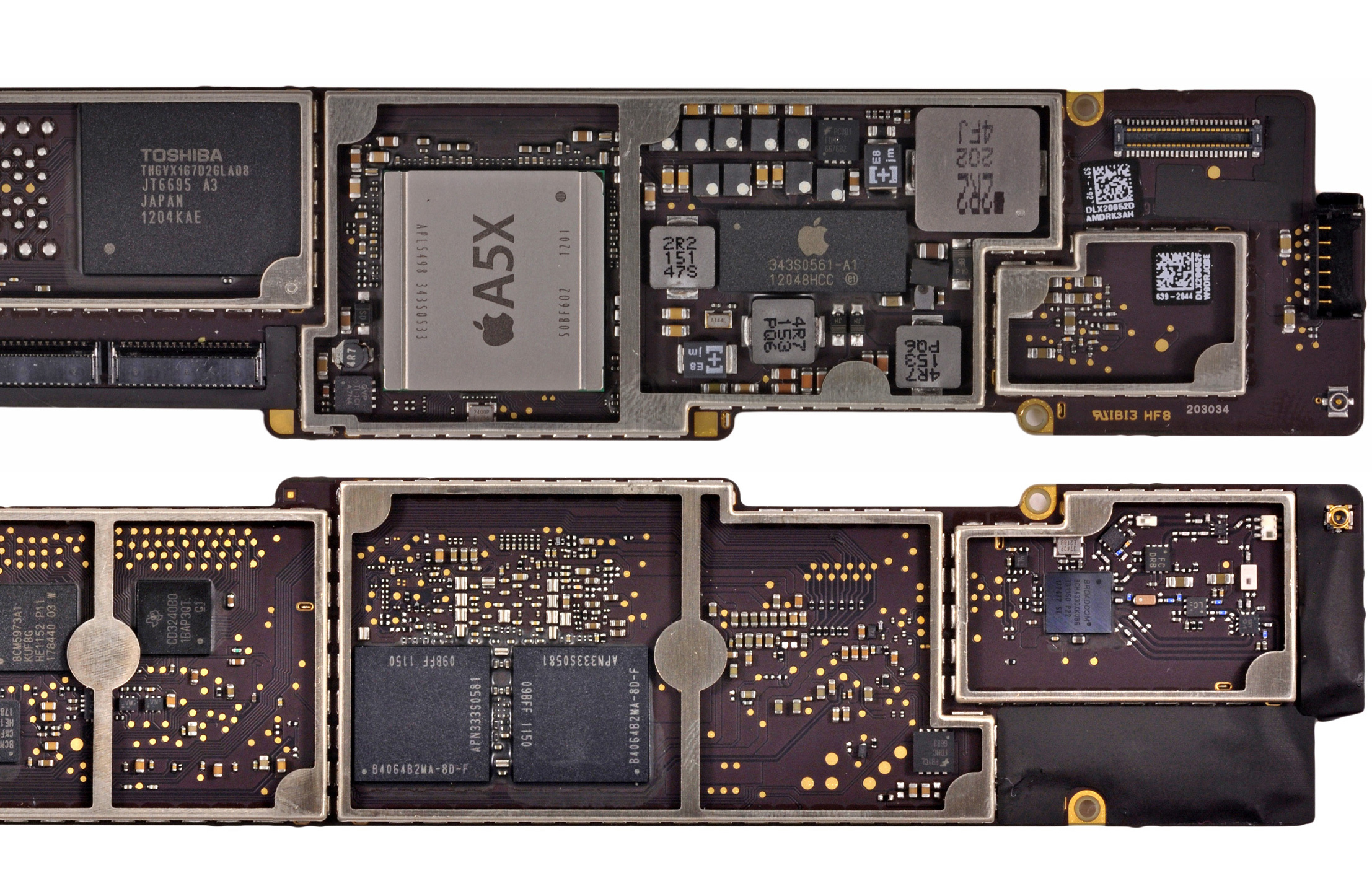
iPad (3rd gen) logic board back (top) and front (bottom), courtesy iFixit
If I'm seeing this correctly, it looks like the DRAM devices are shifted lower than the center point of the A5X. Routing high speed parallel interfaces isn't easy and getting the DRAM as close to the memory controller as possible makes a lot of sense. For years motherboard manufacturers and chipset vendors alike complained about the difficulties of routing a high-speed, 128-bit parallel DRAM interface on a (huge, by comparison) ATX motherboard. What Apple and its partners have achieved here is impressive when you consider that this type of interface only made it to PCs within the past decade.
Looking Forward: 12.8GB/s, the Magical Number
The DRAM speeds in the new iPad haven't changed. The -8D in the Elpida DRAM string tells us this memory is rated at the same 800MHz datarate as what's used in the iPhone 4S and iPad 2. With twice the number of channels to transfer data over however, the total available bandwidth (at least to the GPU) doubles. I brought back the graph I made for our iPhone 4S review to show just how things have improved:
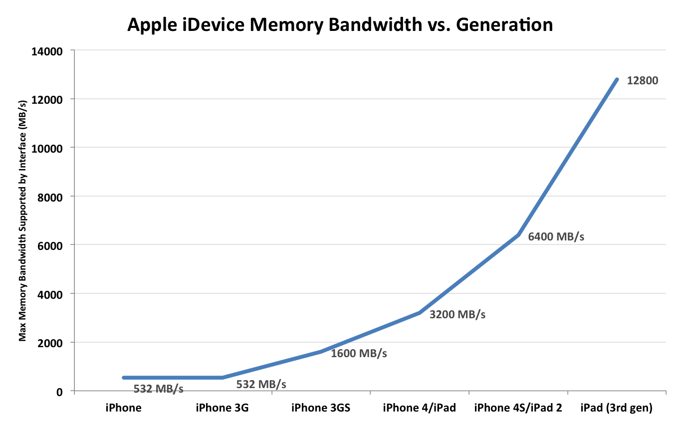
The A5X's memory interface is capable of sending/receiving data at up to 12.8GB/s. While this is still no where near the 100GB/s+ we need for desktop quality graphics at Retina Display resolutions, it's absolutely insane for a mobile SoC. Bandwidth utilization is another story entirely—we have no idea how good Apple's memory controller is (it is designed in-house), but there's 4x the theoretical bandwidth available to the A5X as there is to NVIDIA's Tegra 3.
There's a ton of memory bandwidth here, but Apple got to this point by building a huge, very power hungry SoC. Too power hungry for use in a smartphone. As I mentioned at the start of this article, the SoC alone in the new iPad can consume more power than the entire iPhone 4S (e.g. A5X running Infinity Blade 2 vs. iPhone 4S loading a web page):
| Power Consumption Comparison | ||||
| Apple A5X (SoC + mem interface) | Apple iPhone 4S (entire device) | |||
| Estimated Power Consumption | 2.6W—Infinity Blade 2 | 1.6W—Web Page Loading | ||
There's no question that we need this much (and more) memory bandwidth, but the A5X's route to delivering it is too costly from a standpoint of power. There is a solution to this problem however: Wide IO DRAM.
Instead of using wires to connect DRAM to solder balls on a package that's then stacked on top of your SoC package, Wide IO DRAM uses through-silicon-vias (TSVs) to connect a DRAM die directly to the SoC die. It's an even more costly packaging technique, but the benefits are huge.
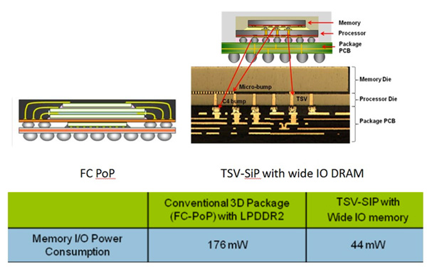
Just as we saw in our discussion of flip-chip vs. wire bonded packages, conventional PoP solutions have limits to how many IO pins you can have in the stack. If you can use the entire silicon surface for direct IO however, you can build some very wide interfaces. It also turns out that these through silicon interfaces are extremely power efficient.
The first Wide IO DRAM spec calls for a 512-bit, 200MHz SDR (single data rate) interface delivering an aggregate of 12.8GB/s of bandwidth. The bandwidth comes at much lower power consumption, while delivering all of the integration benefits of a traditional PoP stack. There are still cooling concerns, but for lower wattage chips they are less worrisome.
Intel originally predicted that by 2015 we'd see 3D die stacking using through-silicon-vias. Qualcomm's roadmaps project usage of TSVs by 2015 as well. The iPhone won't need this much bandwidth in its next generation thanks to a lower resolution display, but when the time comes, there will be a much lower power solution available thanks to Wide IO DRAM.
Oh and 2015 appears to be a very conservative estimate. I'm expecting to see the first Wide IO memory controllers implemented long before then...


234 Comments
View All Comments
Jamezrp - Wednesday, March 28, 2012 - link
Didn't want to cause Verizon too much trouble? Heh, very funny. I am amazed at how the iPad ends up being an amazingly good Wi-Fi hotspot. It almost seems like business users should opt to get an iPad for that function alone. I know plenty of people who would be happy to keep it in their bag, with the hotspot feature enabled constantly, while travelling about. Even for the price there is nothing even close that can compare.Plus, you know, you get the tablet too.
supertwister - Wednesday, March 28, 2012 - link
"It’s a quantum leap from the noisy, 0.7MP mess that was the iPad 2 camera."Interesting choice of word considering a quantum is the smallest possible division for a quantity...
omion - Wednesday, March 28, 2012 - link
Quantum leap:(n) an abrupt change, sudden increase, or dramatic advance
The phrase comes from the ability of particles to make a sudden jump between two energy levels. It is a leap (of any amount) between two quantization levels, not a leap of the smallest possible amount.
drwho9437 - Wednesday, March 28, 2012 - link
A large fraction of the die doesn't seem to have a known use? Wondering what could be taking up all that area if not GPU, CPU and memory interfaces/caches... Most other I/O would have small footprints...tipoo - Wednesday, March 28, 2012 - link
The 4S had a larger than usual die for its voice cancellation features that were needed to make Siri work well, the iPad does't have that but it does have voice dictation so some space is probably for that.PeteH - Wednesday, March 28, 2012 - link
A big chunk of it is probably the ISP they talked about when the 4S debuted.Lucian Armasu - Wednesday, March 28, 2012 - link
So this is how I assumed. The new iPad is in fact slower than the iPad 2, if games actually start using the 2048x1536 resolution for their apps, which everyone seems to be encouraging them to do. But once they do that the graphics will either look poorer, or they will be slower than they were on the old resolution, even on an iPad 2.Add that to the fact that apps are much bigger in size with the retina resolution, and the CPU is the same as last year. The new display might look great, but it's obvious that the new iPad is absolutely a step-back in terms of performance, whether it's GPU or CPU we're talking about. Hardly worth an upgrade, especially for iPad 2 owners.
xype - Thursday, March 29, 2012 - link
Blah blah blah performance blah not worth it.I don’t give a shit about theoretical performance that I might be getting if DNA folding software was available for tablets. I really, really give a shit about being able to read website and ebook text without my eyes straining after an hour.
One would think that 10 years after "No wireless. Less space than a nomad. Lame." and Apple raking in millions and billions of profit, those Geek Metrics™ that people are so fond of here (nothing wrong with that, it’s interesting stuff!), would be recognized as completely and utterly worthless to the average population. But apparently not.
The iPad was never ment to replace PCs and Consoles as a hardcore gaming device, and it was never ment as a render farm server replacement. It would be really nice if people realized that, at some point. In the next 5 years, perhaps.
tipoo - Thursday, March 29, 2012 - link
It seems a bit like the 3GS-4 transition, it used the same GPU despite higher resolution and so performed worse at native, although in this case the CPU is unchanged and the GPU is "only" 2x better for 4x the pixels. Developers got around that on the 4 by making games for the old resolution and using upscaling mode. I'd imagine they will do the same here once games hit the limits of the GPU at native. Games like Infinity Blade 2 also use separate resolutions for things like the menus vs shadows vs terrain textures.darkcrayon - Thursday, March 29, 2012 - link
I guess if the only thing you bought an iPad for were games, and you could only consider a game to be worthwhile if it were drawn directly at 2048x1536, you'd have a point. But of course the new iPad could play games at the "iPad 2" resolution at much higher detail, or at a slightly resolution with the same detail, etc.It doesn't make sense to say it's a step backward in performance overall- it simply has the option to display much higher resolution graphics that the old model didn't have. The iPad 2 displays 2048 x 1536 text at "0 mhz" so to speak. It's not like you are losing anything by having the option of ultra high resolution if the type of game (or app) can use it within the hardware capabilities.