The Apple iPad Review (2012)
by Vivek Gowri & Anand Lal Shimpi on March 28, 2012 3:14 PM ESTA Word on Packaging
Unlike the first two iPads, the 3rd generation iPad abandons the high density flip-chip PoP SoC/DRAM stack and uses a discrete, flip-chip BGA package for the SoC and two discrete BGA packages for the DRAMs.
If you think of SoC silicon as a stack, the lowest layer is where you'll find the actual transistor logic, while the layers of metal above it connect everything together. In the old days, the silicon stack would sit just as I've described it—logic at the bottom, metal layers on top. Pads around the perimeter of the top of the silicon would connect to very thin wires, that would then route to the package substrate and eventually out to balls or pins on the underside of the package. These wire bonded packages, as they were called, had lower limits of how many pins you could have connecting to your chip.
There are also cooling concerns. In a traditional wire bonded package, your cooling solution ultimately rests on a piece of your packaging substrate. The actual silicon itself isn't exposed.
As its name implies, a flip-chip package is literally the inverse of this. Instead of the metal layers being at the top of the stack, before packaging the silicon is inverted and the metal layers are at the bottom of the stack. Solder bumps at the top of the silicon stack (now flipped and at the bottom) connect the topmost metal layer to the package itself. Since we're dealing with solder bumps on the silicon itself rather than wires routed to the edge of the silicon, there's much more surface area for signals to get in/out of the silicon.
Since the chip is flipped, the active logic is now exposed in a flip-chip package and the hottest part of the silicon can be directly attached to a cooling solution.
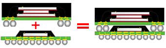
An example of a PoP stack
To save on PCB real estate however, many SoC vendors would take a flip-chip SoC and stack DRAM on top of it in a package-on-package (PoP) configuration. Ultimately this re-introduces many of the problems from older packaging techniques—mainly it becomes difficult to have super wide memory interfaces as your ball-out for the PoP stack is limited to the area around your die, and cooling is a concern once more. For low power, low bandwidth mobile SoCs this hasn't really been a problem, which is why we see PoP stacks deployed all over the place.
Take a look at the A5, a traditional FC-BGA SoC with PoP DRAM vs. the A5X (this isn't to scale):
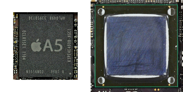
Images courtesy iFixit
The A5X in this case is a FC-BGA SoC but without any DRAM stacked on top of it. The A5X is instead covered in a thermally conductive paste and then with a metallic heatspreader to conduct heat away from the SoC and protect the silicon.
Given the size and complexity of the A5X SoC, it's no surprise that Apple didn't want to insulate the silicon with a stack of DRAM on top of it. In typical package-on-package stacks, you'd see solder bumps around the silicon, on the package itself, that a separate DRAM package would adhere to. Instead of building up a PoP stack here, Apple simply located its two 64-bit DRAM devices on the opposite side of the iPad's logic board and routed the four 32-bit LP-DDR2 memory channels through the PCB layers.
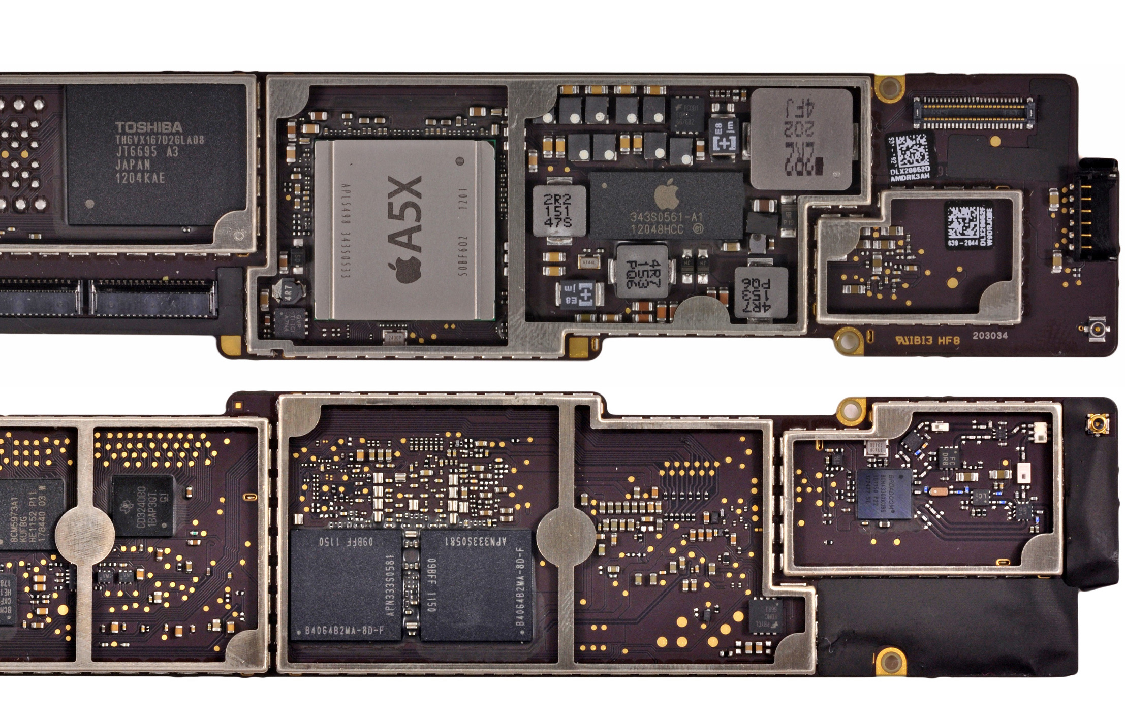
iPad (3rd gen) logic board back (top) and front (bottom), courtesy iFixit
If I'm seeing this correctly, it looks like the DRAM devices are shifted lower than the center point of the A5X. Routing high speed parallel interfaces isn't easy and getting the DRAM as close to the memory controller as possible makes a lot of sense. For years motherboard manufacturers and chipset vendors alike complained about the difficulties of routing a high-speed, 128-bit parallel DRAM interface on a (huge, by comparison) ATX motherboard. What Apple and its partners have achieved here is impressive when you consider that this type of interface only made it to PCs within the past decade.
Looking Forward: 12.8GB/s, the Magical Number
The DRAM speeds in the new iPad haven't changed. The -8D in the Elpida DRAM string tells us this memory is rated at the same 800MHz datarate as what's used in the iPhone 4S and iPad 2. With twice the number of channels to transfer data over however, the total available bandwidth (at least to the GPU) doubles. I brought back the graph I made for our iPhone 4S review to show just how things have improved:
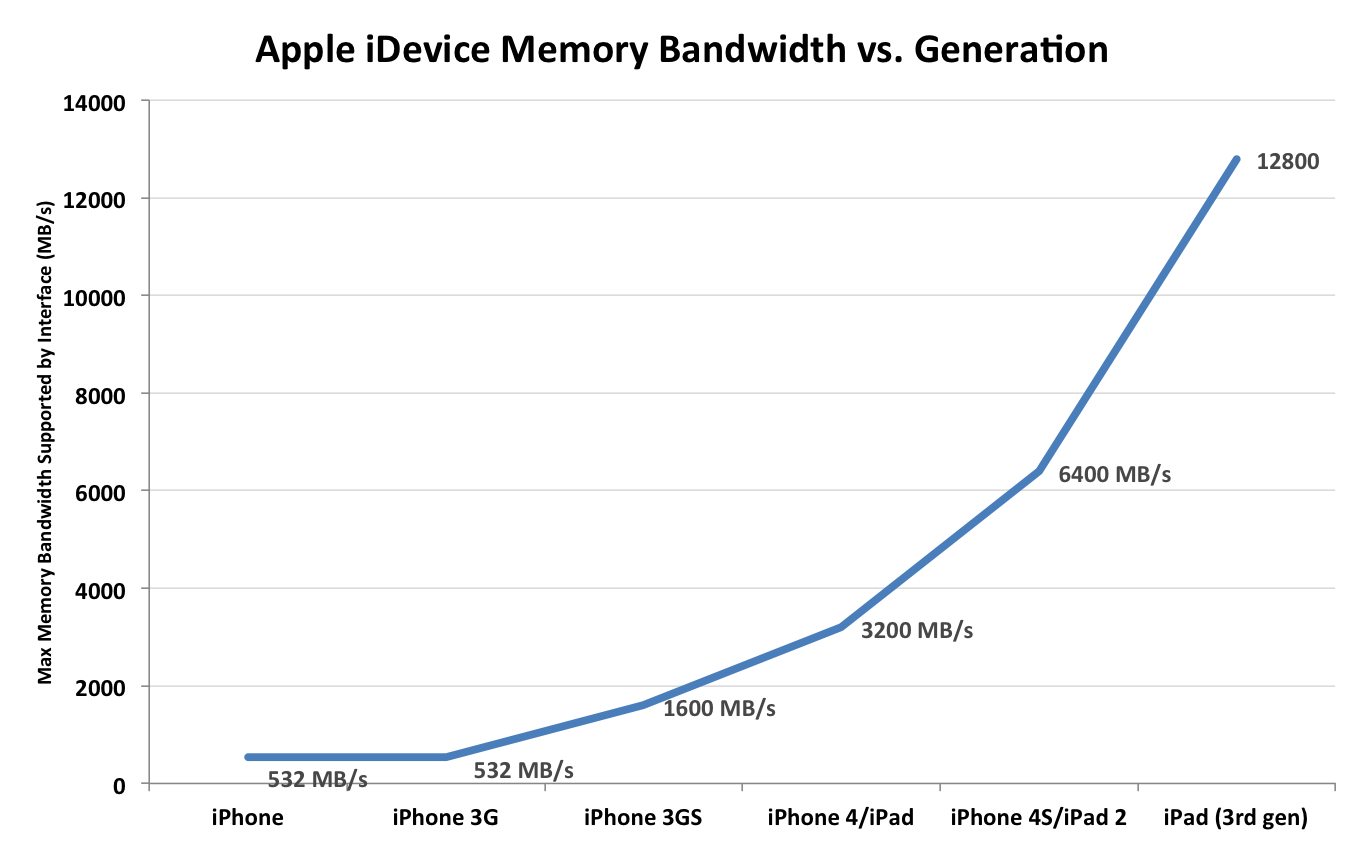
The A5X's memory interface is capable of sending/receiving data at up to 12.8GB/s. While this is still no where near the 100GB/s+ we need for desktop quality graphics at Retina Display resolutions, it's absolutely insane for a mobile SoC. Bandwidth utilization is another story entirely—we have no idea how good Apple's memory controller is (it is designed in-house), but there's 4x the theoretical bandwidth available to the A5X as there is to NVIDIA's Tegra 3.
There's a ton of memory bandwidth here, but Apple got to this point by building a huge, very power hungry SoC. Too power hungry for use in a smartphone. As I mentioned at the start of this article, the SoC alone in the new iPad can consume more power than the entire iPhone 4S (e.g. A5X running Infinity Blade 2 vs. iPhone 4S loading a web page):
| Power Consumption Comparison | ||||
| Apple A5X (SoC + mem interface) | Apple iPhone 4S (entire device) | |||
| Estimated Power Consumption | 2.6W—Infinity Blade 2 | 1.6W—Web Page Loading | ||
There's no question that we need this much (and more) memory bandwidth, but the A5X's route to delivering it is too costly from a standpoint of power. There is a solution to this problem however: Wide IO DRAM.
Instead of using wires to connect DRAM to solder balls on a package that's then stacked on top of your SoC package, Wide IO DRAM uses through-silicon-vias (TSVs) to connect a DRAM die directly to the SoC die. It's an even more costly packaging technique, but the benefits are huge.
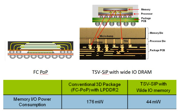
Just as we saw in our discussion of flip-chip vs. wire bonded packages, conventional PoP solutions have limits to how many IO pins you can have in the stack. If you can use the entire silicon surface for direct IO however, you can build some very wide interfaces. It also turns out that these through silicon interfaces are extremely power efficient.
The first Wide IO DRAM spec calls for a 512-bit, 200MHz SDR (single data rate) interface delivering an aggregate of 12.8GB/s of bandwidth. The bandwidth comes at much lower power consumption, while delivering all of the integration benefits of a traditional PoP stack. There are still cooling concerns, but for lower wattage chips they are less worrisome.
Intel originally predicted that by 2015 we'd see 3D die stacking using through-silicon-vias. Qualcomm's roadmaps project usage of TSVs by 2015 as well. The iPhone won't need this much bandwidth in its next generation thanks to a lower resolution display, but when the time comes, there will be a much lower power solution available thanks to Wide IO DRAM.
Oh and 2015 appears to be a very conservative estimate. I'm expecting to see the first Wide IO memory controllers implemented long before then...


234 Comments
View All Comments
doobydoo - Saturday, March 31, 2012 - link
Lucian Armasu, you talk the most complete nonsense of anyone I've ever seen on here.The performance is not worse, by any stretch of the imagination, and lets remember that the iPad 2 runs rings around the Android competition graphically anyway. If you want to run the same game at the same resolution, which wont look worse, at all (it would look exactly the same) it will run at 2x the FPS or more (up-scaled). Alternatively, for games for which it is beneficial, you can quadruple the quality and still run the game at perfectly acceptable FPS, since the game will be specifically designed to run on that device. Attempting anything like that quality on any other tablet is not only impossible by virtue of their inferior screens, they don't have the necessary GPU either.
In other words, you EITHER have a massive improvement in quality, or a massive improvement in performance, over a device (iPad 2) which was still the fastest performing GPU tablet even a year after it came out. The game developers get to make this decision - so they just got 2 great new options on a clearly much more powerful device. To describe that as not worth an upgrade is quite frankly ludicrous, you have zero credibility from here on in.
thejoelhansen - Wednesday, March 28, 2012 - link
Hey Anand,First of all - thank you so much for the quality reviews and benchmarks. You've helped me build a number of servers and gaming rigs. :)
Secondly, I'm not sure I know what you mean when you state that "Prioritizing GPU performance over a CPU upgrade is nothing new for Apple..." (Page 11).
The only time I can remember Apple doing so is when keeping the 13" Macbook/ MBPs on C2Ds w/ Nvidia until eventually relying on Intel's (still) anemic "HD" graphics... Is that what you're referring to?
I seem to remember Apple constantly ignoring the GPU in favor of CPU upgrades, other than that one scenario... Could be mistaken. ;)
And again - thanks for the great reviews! :)
AnnonymousCoward - Wednesday, March 28, 2012 - link
"Retina Display" is a stupid name. Retinas sense light, which the display doesn't do.xype - Thursday, March 29, 2012 - link
GeForce is a stupid name, as the video cards don’t have anything to do with influencing the gravitational acceleration of an object or anything close to that.Retina Display sounds fancy and is lightyears ahead of "QXGA IPS TFT Panel" when talking about it. :P
Sabresiberian - Thursday, March 29, 2012 - link
While I agree that "Retina Display" is a cool enough sounding name, and that's pretty much all you need for a product, unless it's totally misleading, it's not an original use of the phrase. The term has been used in various science fiction stories and tends to mean a display device that projects an image directly onto the retina.I always thought of "GeForce" as being an artist's licensed reference to the cards being a Force in Graphics, so the name had a certain logic behind it.
;)
seapeople - Tuesday, April 3, 2012 - link
Wait, so "Retina Display" gets you in a tizzy but "GeForce" makes perfect sense to you? You must have interesting interactions in everyday life.ThreeDee912 - Thursday, March 29, 2012 - link
It's basically the same concept with Gorilla Glass or UltraSharp displays. It obviously doesn't mean that Corning makes glass out of gorillas, or that Dell will cut your eyes out and put them on display. It's just a marketing name.SR81 - Saturday, March 31, 2012 - link
Funny I always believed the "Ge" was short for geometry. Whatever the case you can blame the name on the fans who came up with it.tipoo - Thursday, March 29, 2012 - link
iPad is a stupid name. Pads collect blood from...Well, never mind. But since when are names always literal?doobydoo - Saturday, March 31, 2012 - link
What would you call a display which had been optimised for use by retinas?Retina display.
They aren't saying the display IS a retina, they are saying it is designed with retinas in mind.
The scientific point is very clear and as such I don't think the name is misleading at all. The point is the device has sufficient PPI at typical viewing distance that a person with typical eyesight wont be able to discern the individual pixels.
As it happens, strictly speaking, the retina itself is capable of discerning more pixels at typical viewing distance than the PPI of the new iPad, but the other elements of the human eye introduce loss in the quality of the image which is then ultimately sent on to the brain. While scientifically this is a distinction, to end consumers it is a distinction without a difference, so the name makes sense in my opinion.