The Apple iPad Review (2012)
by Vivek Gowri & Anand Lal Shimpi on March 28, 2012 3:14 PM ESTA Word on Packaging
Unlike the first two iPads, the 3rd generation iPad abandons the high density flip-chip PoP SoC/DRAM stack and uses a discrete, flip-chip BGA package for the SoC and two discrete BGA packages for the DRAMs.
If you think of SoC silicon as a stack, the lowest layer is where you'll find the actual transistor logic, while the layers of metal above it connect everything together. In the old days, the silicon stack would sit just as I've described it—logic at the bottom, metal layers on top. Pads around the perimeter of the top of the silicon would connect to very thin wires, that would then route to the package substrate and eventually out to balls or pins on the underside of the package. These wire bonded packages, as they were called, had lower limits of how many pins you could have connecting to your chip.
There are also cooling concerns. In a traditional wire bonded package, your cooling solution ultimately rests on a piece of your packaging substrate. The actual silicon itself isn't exposed.
As its name implies, a flip-chip package is literally the inverse of this. Instead of the metal layers being at the top of the stack, before packaging the silicon is inverted and the metal layers are at the bottom of the stack. Solder bumps at the top of the silicon stack (now flipped and at the bottom) connect the topmost metal layer to the package itself. Since we're dealing with solder bumps on the silicon itself rather than wires routed to the edge of the silicon, there's much more surface area for signals to get in/out of the silicon.
Since the chip is flipped, the active logic is now exposed in a flip-chip package and the hottest part of the silicon can be directly attached to a cooling solution.
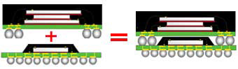
An example of a PoP stack
To save on PCB real estate however, many SoC vendors would take a flip-chip SoC and stack DRAM on top of it in a package-on-package (PoP) configuration. Ultimately this re-introduces many of the problems from older packaging techniques—mainly it becomes difficult to have super wide memory interfaces as your ball-out for the PoP stack is limited to the area around your die, and cooling is a concern once more. For low power, low bandwidth mobile SoCs this hasn't really been a problem, which is why we see PoP stacks deployed all over the place.
Take a look at the A5, a traditional FC-BGA SoC with PoP DRAM vs. the A5X (this isn't to scale):
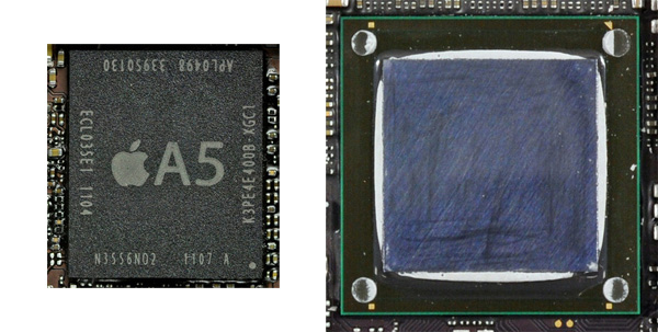
Images courtesy iFixit
The A5X in this case is a FC-BGA SoC but without any DRAM stacked on top of it. The A5X is instead covered in a thermally conductive paste and then with a metallic heatspreader to conduct heat away from the SoC and protect the silicon.
Given the size and complexity of the A5X SoC, it's no surprise that Apple didn't want to insulate the silicon with a stack of DRAM on top of it. In typical package-on-package stacks, you'd see solder bumps around the silicon, on the package itself, that a separate DRAM package would adhere to. Instead of building up a PoP stack here, Apple simply located its two 64-bit DRAM devices on the opposite side of the iPad's logic board and routed the four 32-bit LP-DDR2 memory channels through the PCB layers.
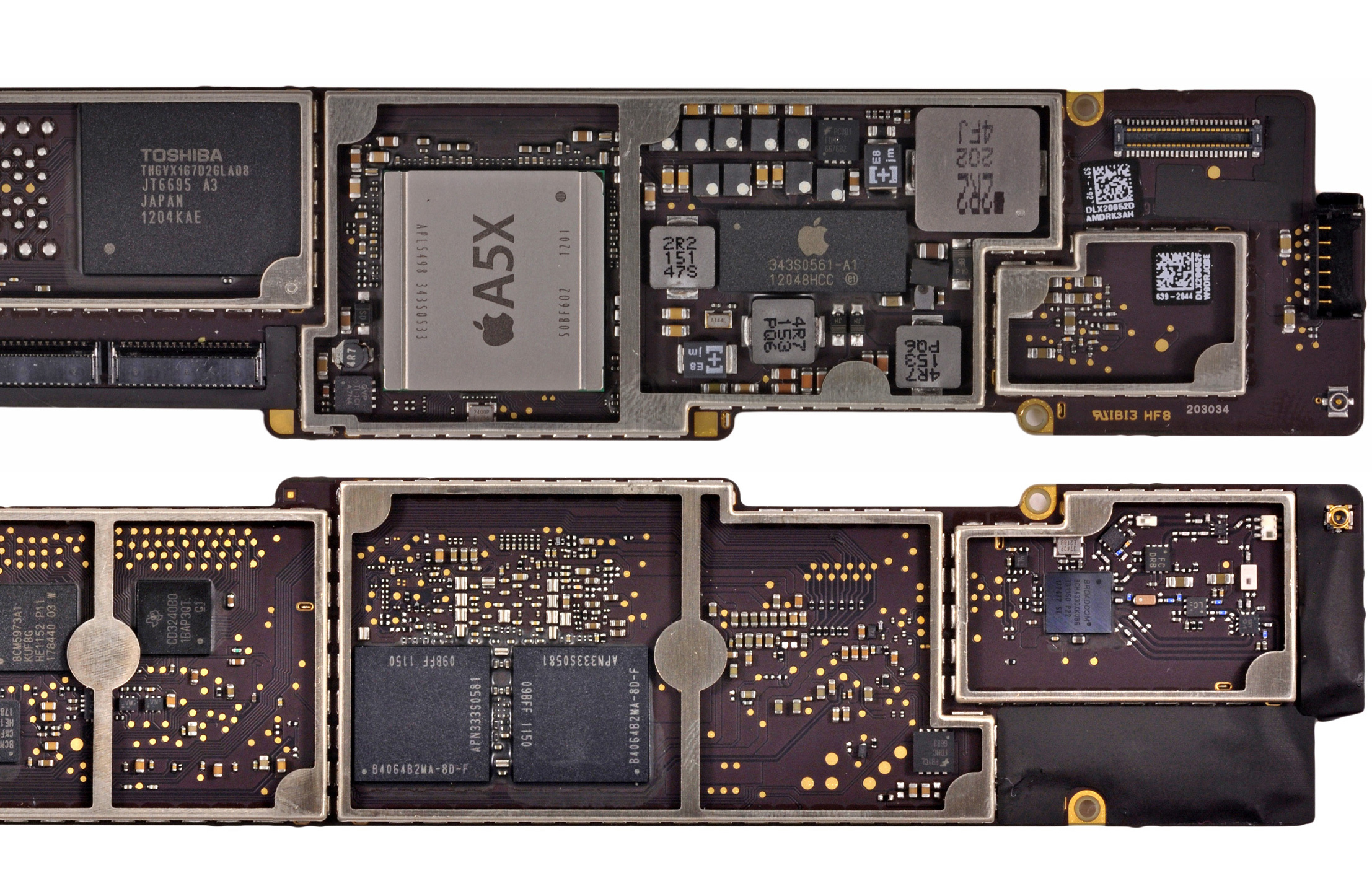
iPad (3rd gen) logic board back (top) and front (bottom), courtesy iFixit
If I'm seeing this correctly, it looks like the DRAM devices are shifted lower than the center point of the A5X. Routing high speed parallel interfaces isn't easy and getting the DRAM as close to the memory controller as possible makes a lot of sense. For years motherboard manufacturers and chipset vendors alike complained about the difficulties of routing a high-speed, 128-bit parallel DRAM interface on a (huge, by comparison) ATX motherboard. What Apple and its partners have achieved here is impressive when you consider that this type of interface only made it to PCs within the past decade.
Looking Forward: 12.8GB/s, the Magical Number
The DRAM speeds in the new iPad haven't changed. The -8D in the Elpida DRAM string tells us this memory is rated at the same 800MHz datarate as what's used in the iPhone 4S and iPad 2. With twice the number of channels to transfer data over however, the total available bandwidth (at least to the GPU) doubles. I brought back the graph I made for our iPhone 4S review to show just how things have improved:
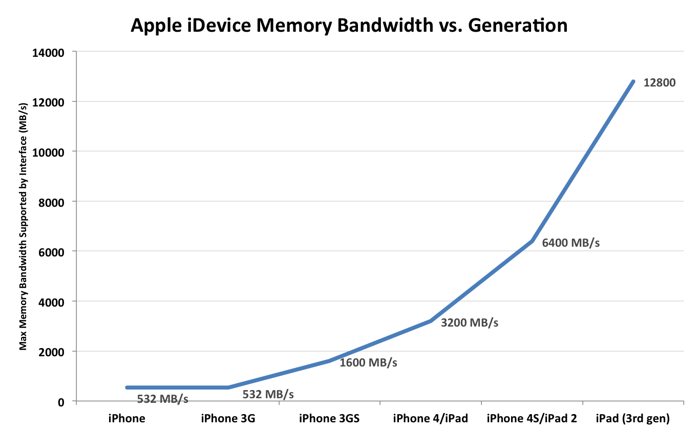
The A5X's memory interface is capable of sending/receiving data at up to 12.8GB/s. While this is still no where near the 100GB/s+ we need for desktop quality graphics at Retina Display resolutions, it's absolutely insane for a mobile SoC. Bandwidth utilization is another story entirely—we have no idea how good Apple's memory controller is (it is designed in-house), but there's 4x the theoretical bandwidth available to the A5X as there is to NVIDIA's Tegra 3.
There's a ton of memory bandwidth here, but Apple got to this point by building a huge, very power hungry SoC. Too power hungry for use in a smartphone. As I mentioned at the start of this article, the SoC alone in the new iPad can consume more power than the entire iPhone 4S (e.g. A5X running Infinity Blade 2 vs. iPhone 4S loading a web page):
| Power Consumption Comparison | ||||
| Apple A5X (SoC + mem interface) | Apple iPhone 4S (entire device) | |||
| Estimated Power Consumption | 2.6W—Infinity Blade 2 | 1.6W—Web Page Loading | ||
There's no question that we need this much (and more) memory bandwidth, but the A5X's route to delivering it is too costly from a standpoint of power. There is a solution to this problem however: Wide IO DRAM.
Instead of using wires to connect DRAM to solder balls on a package that's then stacked on top of your SoC package, Wide IO DRAM uses through-silicon-vias (TSVs) to connect a DRAM die directly to the SoC die. It's an even more costly packaging technique, but the benefits are huge.
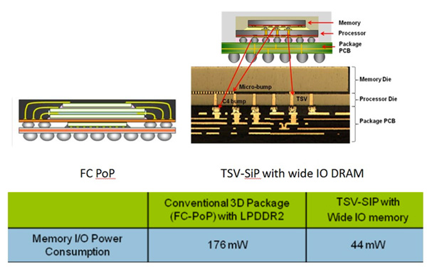
Just as we saw in our discussion of flip-chip vs. wire bonded packages, conventional PoP solutions have limits to how many IO pins you can have in the stack. If you can use the entire silicon surface for direct IO however, you can build some very wide interfaces. It also turns out that these through silicon interfaces are extremely power efficient.
The first Wide IO DRAM spec calls for a 512-bit, 200MHz SDR (single data rate) interface delivering an aggregate of 12.8GB/s of bandwidth. The bandwidth comes at much lower power consumption, while delivering all of the integration benefits of a traditional PoP stack. There are still cooling concerns, but for lower wattage chips they are less worrisome.
Intel originally predicted that by 2015 we'd see 3D die stacking using through-silicon-vias. Qualcomm's roadmaps project usage of TSVs by 2015 as well. The iPhone won't need this much bandwidth in its next generation thanks to a lower resolution display, but when the time comes, there will be a much lower power solution available thanks to Wide IO DRAM.
Oh and 2015 appears to be a very conservative estimate. I'm expecting to see the first Wide IO memory controllers implemented long before then...


234 Comments
View All Comments
Riseofthefootclan - Thursday, March 29, 2012 - link
I entered the tablet market this year in hopes of enhancing my school experience. I was looking for a device that would do the following: reading textbooks, slides, notes, watching video etc.I too looked at the kindle, but I will tell you now that for what you want I'd avoid it.
I first purchased a Samsung galaxy tab 10.1 LTE. I wanted Internet every where I went, but soon became frustrated with the android operating system (inconsistently chunky etc).
After playing with an iPad 2 in the store, I realized it was a much better experience. Fluid and problem free.
A month later the iPad 3 (new iPad) is released. After playing with it I realized how much better the screen was, and how much that impacted the experience (especially for someone who primarily uses the device for text consumption).
So now, here I sit, with a 32b LTE iPad 3. I don't regret the purchase one bit. Armed with the Bluetooth keyboard, or just the on screen variant, I can also take notes quite competently (wrote this entire thing out with the on screen keyboard).
Best educational tool I have ever purchased. In my hands I can carry my one stop shop for web browsing, email, textbooks, fictional books, course materials, lectures and even games.
Coming from an iPad 2, I'd go so far as to say it was well worth the upgrade.
I highly recommend picking one of these up, as I believe it will fit your bill of requirements to a tee.
adityarjun - Thursday, March 29, 2012 - link
Thanks dude! And all others who replied. I guess I will be picking up a 32gb LTE version of the ipad.Do you guys know whether the ipad has international warranty? If I were to buy it from the US and import it here, would I have warranty?
And how many years of warranty does it have? Is it a replacement warranty, i.e. , if anything is broken they give a new ipad or a normal warranty?
This is another aspect the review didnt cover. A para detailing the warranty and tech support should have been there imo.
adityarjun - Thursday, March 29, 2012 - link
Oops forgot to add this in the comment above-- which keyboard are you using.. I think I will pick the Logitech one.And any good stylus?
Also, for protection I guess I will go with a Zagg shield and the smart cover. Will that be enough?
OCedHrt - Thursday, March 29, 2012 - link
How come the review starts with the 10.1-inch 1920 x 1200 Super IPS+ tablet but all the comparisons are with the 1280 x 800 tablet?adityarjun - Thursday, March 29, 2012 - link
I am not sure but I dont think that those tablets are in the market yet. That was just a comparison of specs. Later on we had a comparison with other major tablets available in the market currently.i.e ipad 2 and the transformer prime.OCedHrt - Thursday, March 29, 2012 - link
Says 40 nm on page 2 and 45 nm on page 6.g1011999 - Thursday, March 29, 2012 - link
At Page (The A5X SoC) / Table (ARM Cortex A9 Based SoC Comparison)The cell for "A5X" and "Memory Interface to the CPU" shall be "Quad channel(128bit)"
Ryan Smith - Thursday, March 29, 2012 - link
Actually that's correct as it stands. The memory interface to the CPU is 64bit on the A5X. The other two memory channels go to the GPU, rather than the CPU.g1011999 - Thursday, March 29, 2012 - link
No, Those memory controllers are multi-port AXI controller which are connected to L2 cache controller, system fabrics, GPU.L2 cache controller is connected to all those 128bit dram controller, either through direct connection (memory adapter like omap 4470) or through system AXI bus, so the cpu can access all the memory.
The A5X is a SoC coupled with 128bit quad channel DRAM regardless whether the bandwidth from CPU(L2 cache) to memory is sufficient or not.
The IPs ( CPU, video codec, display controller, GPU, CAM-IF ...) on SoC can take advantage from the 128bit memory interface with less chance of congestion.
PeteH - Friday, March 30, 2012 - link
And how do you know the internal system bus is AXI?