AMD's Radeon HD 6970 & Radeon HD 6950: Paving The Future For AMD
by Ryan Smith on December 15, 2010 12:01 AM ESTCayman: The Last 32nm Castaway
With the launch of the Barts GPU and the 6800 series, we touched on the fact that AMD was counting on the 32nm process to give them a half-node shrink to take them in to 2011. When TSMC fell behind schedule on the 40nm process, and then the 32nm process before canceling it outright, AMD had to start moving on plans for a new generation of 40nm products instead.
The 32nm predecessor of Barts was among the earlier projects to be sent to 40nm. This was due to the fact that before 32nm was even canceled, TSMC’s pricing was going to make 32nm more expensive per transistor than 40nm, a problem for a mid-range part where AMD has specific margins they’d like to hit. Had Barts been made on the 32nm process as projected, it would have been more expensive to make than on the 40nm process, even though the 32nm version would be smaller. Thus 32nm was uneconomical for gaming GPUs, and Barts was moved to the 40nm process.
Cayman on the other hand was going to be a high-end part. Certainly being uneconomical is undesirable, but high-end parts carry high margins, especially if they can be sold in the professional market as compute products (just ask NVIDIA). As such, while Barts went to 40nm, Cayman’s predecessor stayed on the 32nm process until the very end. The Cayman team did begin planning to move back to 40nm before TSMC officially canceled the 32nm process, but if AMD had a choice at the time they would have rather had Cayman on the 32nm process.
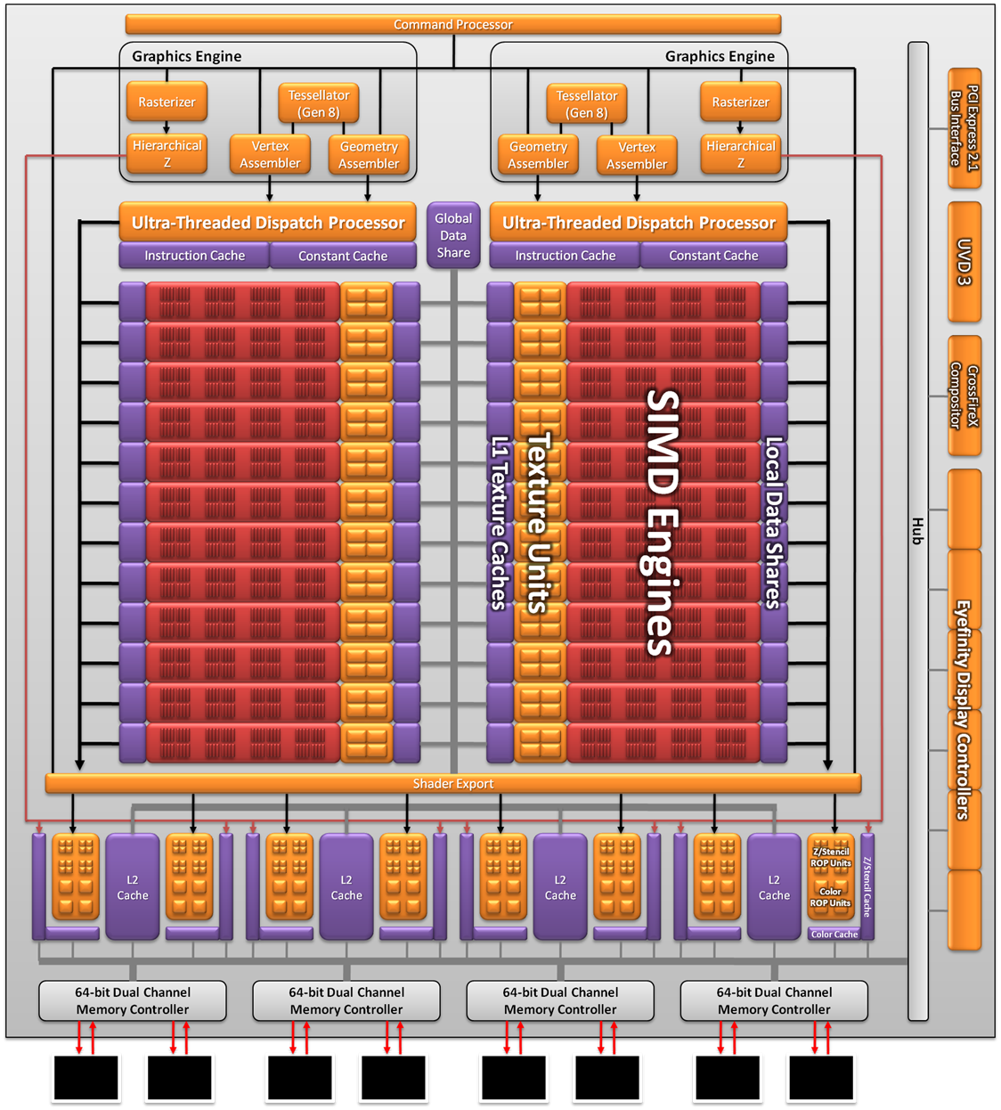
As a result the Cayman we’re seeing today is not what AMD originally envisioned as a 32nm part. AMD won’t tell us everything that they had to give up to create the 40nm Cayman (there has to be a few surprises for 28nm) but we do know a few things. First and foremost was size; AMD’s small die strategy is not dead, but getting the boot from the 32nm process does take the wind out of it. At 389mm2 Cayman is the largest AMD GPU since the disastrous R600, and well off the sub-300mm2 size that the small die strategy dictates. In terms of efficient usage of space though AMD is doing quite well; Cayman has 2.64 billion transistors, 500mil more than Cypress. AMD was able to pack 29% more transistors in only 16% more space.
Even then, just reaching that die size is a compromise between features and production costs. AMD didn’t simply settle for a larger GPU, but they had to give up some things to keep it from being even larger. SIMDs were on the chopping block; 32nm Cayman would have had more SIMDs for more performance. Features were also lost, and this is where AMD is keeping mum. We know PCI Express 3.0 functionality was scheduled for the 32nm part, where AMD had to give up their PCIe 3.0 controller for a smaller 2.1 controller to make up for their die size difference. This in all honesty may have worked out better for them: PCIe 3.0 ended up being delayed until November, so suitable motherboards are still at least months away.
The end result is that Cayman as we know it is a compromise to make it happen on 40nm. AMD got their new VLIW4 architecture, but they had to give up performance and an unknown number of features to get there. On the flip side this will make 28nm all the more interesting, as we’ll get to see many of the features that were supposed to make it for 2010 but never arrived.


168 Comments
View All Comments
B3an - Thursday, December 16, 2010 - link
Very stupid uninformed and narrow-minded comment. People like you never look to the future which anyone should do when buying a graphics card, and you completely lack any imagination. Theres already tons of uses for GPU computing, many of which the average computer user can make use of, even if it's simply encoding a video faster. And it will be use a LOT more in the future.Most people, especially ones that game, dont even have 17" monitors these days. The average size monitor for any new computer is at least 21" with 1680 res these days. Your whole comment is as if everyone has the exact same needs as YOU. You might be happy with your ridiculously small monitor, and playing games at low res on lower settings, and it might get the job done, but lots of people dont want this, they have standards and large monitors and needs to make use of these new GPU's. I cant exactly see many people buying these cards with a 17" monitor!
CeepieGeepie - Thursday, December 16, 2010 - link
Hi Ryan,First, thanks for the review. I really appreciate the detail and depth on the architecture and compute capabilities.
I wondered if you had considered using some of the GPU benchmarking suites from the academic community to give even more depth for compute capability comparisons. Both SHOC (http://ft.ornl.gov/doku/shoc/start) and Rodinia (https://www.cs.virginia.edu/~skadron/wiki/rodinia/... look like they might provide a very interesting set of benchmarks.
Ryan Smith - Thursday, December 16, 2010 - link
Hi Ceepie;I've looked in to SHOC before. Unfortunately it's *nix-only, which means we can't integrate it in to our Windows-based testing environment. NVIDIA and AMD both work first and foremost on Windows drivers for their gaming card launches, so we rarely (if ever) have Linux drivers available for the launch.
As for Rodinia, this is the first time I've seen it. But it looks like their OpenCL codepath isn't done, which means it isn't suitable for cross-vendor comparisons right now.
IdBuRnS - Thursday, December 16, 2010 - link
"So with that in mind a $370 launch price is neither aggressive nor overpriced. Launching at $20 over the GTX 570 isn’t going to start a price war, but it’s also not so expensive to rule the card out. "At NewEgg right now:
Cheapest GTX 570 - $509
Cheapest 6970 - $369
$30 difference? What are you smoking? Try $140 difference.
IdBuRnS - Thursday, December 16, 2010 - link
Oops, $20 difference. Even worse.IdBuRnS - Thursday, December 16, 2010 - link
570...not 580.../hangsheadinshame
epyon96 - Thursday, December 16, 2010 - link
This was a very interesting discussion to me in the article.I'm curious if Anandtech might expand on this further in a future dedicated article comparing what NVIDIA is using to AMD.
Are they also more similar to VLIW4 or VLIW5?
Can someone else shed some light on it?
Ryan Smith - Thursday, December 16, 2010 - link
We wrote something almost exactly like you're asking for for our Radeon HD 4870 review.http://www.anandtech.com/show/2556
AMD and NVIDIA's compute architectures are still fundamentally the same, so just about everything in that article still holds true. The biggest break is VLIW4 for the 6900 series, which we covered in our article this week.
But to quickly answer your question, GF100/GF110 do not immediately compare to VLIW4 or VLIW5. NVIDIA is using a pure scalar architecture, which has a number of fundamental differences from any VLIW architecture.
dustcrusher - Thursday, December 16, 2010 - link
The cheap insults are nothing but a detriment to what is otherwise an interesting argument, even if I don't agree with you.As far as the intellect of Anandtech readers goes, this is one of the few sites where almost all of the comments are worth reading; most sites are the opposite- one or two tiny bits of gold in a big pan of mud.
I'm not going to "vastly overestimate" OR underestimate your intellect though- instead I'm going to assume that you got caught up in the moment. This isn't Tom's or Dailytech, a little snark is plenty.
Arnulf - Thursday, December 16, 2010 - link
When you launch an application (say a game), it is likely to be the only active thread running on the system, or perhaps one of very few active threads. CPU with Turbo function will clock up as high as possible to run this main thread. When further threads are launched by the application, CPU will inevitably increase its power consumption and consequently clock down.While CPU manufacturers don't advertise this functionality in this manner, it is really no different from PowerTune.
Would PowerTune technology make you feel any better if it was marketed the other way around, the way CPUs are ? (mentioning lowest frequencies and clock boost provided that thermal cap isn't met yet)