Intel's Sandy Bridge Architecture Exposed
by Anand Lal Shimpi on September 14, 2010 4:10 AM EST- Posted in
- CPUs
- Intel
- Sandy Bridge
Sandy Bridge Graphics
The largest performance improvement on Sandy Bridge vs. current Westmere architectures actually has nothing to do with the CPU, it’s all graphics. While the CPU cores show a 10 - 30% improvement in performance, Sandy Bridge graphics performance is easily double what Intel delivered with Clarkdale/Arrandale at the beginning of the year.
While the ‘dales improved performance by moving graphics to a 45nm process, increasing shader hardware and clock speed, SNB graphics improves through a significant increase in IPC.
The Sandy Bridge GPU is on-die built out of the same 32nm transistors as the CPU cores. The GPU is on its own power island and clock domain. The GPU can be powered down or clocked up independently of the CPU. Graphics turbo is available on both desktop and mobile parts, and you get more bins with graphics turbo on Sandy Bridge than you did with Arrandale.
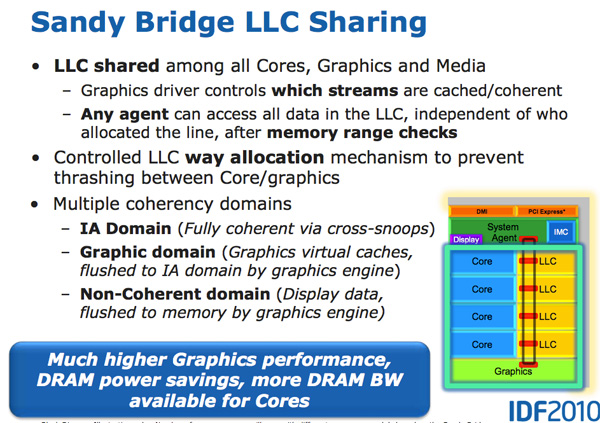
The GPU is treated like an equal citizen in the Sandy Bridge world, it gets equal access to the L3 cache. The graphics driver controls what gets into the L3 cache and you can even limit how much cache the GPU is able to use. Storing graphics data in the cache is particularly important as it saves trips to main memory which are costly from both a performance and power standpoint. Redesigning a GPU to make use of a cache isn’t a simple task. It usually requires the sort of complete re-design that NVIDIA did with GF100 for example.
SNB graphics is the anti-Larrabee. While Larrabee focused on extensive use of fully programmable hardware (with the exception of the texture hardware), SNB graphics (internally referred to as Gen 6 graphics) makes extensive use of fixed function hardware. The design mentality was anything that could be described by a fixed function should be implemented in fixed function hardware. The benefit is performance/power/die area efficiency, at the expense of flexibility. Keeping much of the GPU fixed function is in-line with Intel’s CPU centric view of the world. By contrast, taking the GPU as programmable as possible makes more sense for a GPU focused company like NVIDIA.
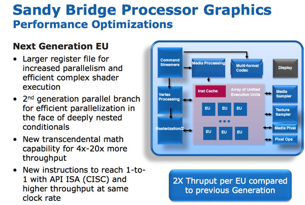
The programmable shader hardware is composed of shaders/cores/execution units that Intel calls EUs. Each EU can dual issue picking instructions from multiple threads. The internal ISA maps one-to-one with most DirectX 10 API instructions resulting in a very CISC-like architecture. Moving to one-to-one API to instruction mapping increases IPC by effectively increasing the width of the EUs.
There are other improvements within the EU. Transcendental math is handled by hardware in the EU and its performance has been sped up considerably. Intel told us that sine and cosine operations are several orders of magnitude faster now than they were in current HD Graphics.
In previous Intel graphics architectures the register file was repartitioned on the fly. If a thread needed fewer registers, the remaining registers could be allocated to another thread. While this was a great approach for saving die area, it proved to be a limiter for performance. In many cases threads couldn’t be worked on as there were no registers available for use. Prior to Intel HD Graphics each thread had an average of 64 registers, the ‘dales brought that average up to 80 per thread. In SNB, the GPU has a fixed amount of registers per thread: 120. The register count limiting thread count scenarios have been alleviated.
All of these enhancements result in 2x the instruction throughput per EU compared to Intel’s HD Graphics today.

Sandy Bridge vs. NVIDIA GeForce 310M Playing Starcraft 2
At launch there will be two versions of Sandy Bridge graphics: one with 6 EUs and one with 12 EUs. All mobile parts (at launch) will use 12 EUs, while desktop SKUs may either use 6 or 12 depending on the model. From what I’ve heard, the higher end SKUs may have 12 while the lower end models will have 6 but I haven’t seen it on a roadmap yet so I can’t confirm. With a 2x improvement in throughput per EU, you should see greater than Intel HD Graphics performance even with the 6 EU parts (thanks to higher clock speeds and the GPU sharing the L3 cache).


62 Comments
View All Comments
markhennry - Monday, November 29, 2010 - link
wow awesome site about the computer parts i thinking buy a cpu and now i got a good help from this sites..katleo123 - Tuesday, February 1, 2011 - link
It is not expected to compete Core i7 processors to take its place
visit http://www.techreign.com/2010/12/intels-sandy-brid...