The RV870 Story: AMD Showing up to the Fight
by Anand Lal Shimpi on February 14, 2010 12:00 AM EST- Posted in
- GPUs
The Payoff: How RV740 Saved Cypress
For its first 40nm GPU, ATI chose the biggest die that made sense in its roadmap. That was the RV740 (Radeon HD 4770):
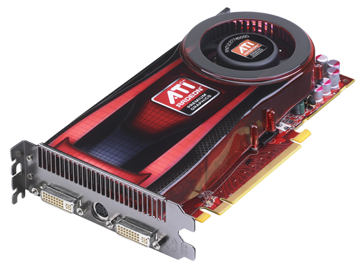
The first to 40nm - The ATI Radeon HD 4770, April 2009
NVIDIA however picked a smaller die. While the RV740 was a 137mm2 GPU, NVIDIA’s first 40nm parts were the G210 and GT220 which measured 57mm2 and 100mm2. The G210 and GT220 were OEM-only for the first months of their life, and I’m guessing the G210 made up a good percentage of those orders. Note that it wasn’t until the release of the GeForce GT 240 that NVIDIA made a 40nm die equal in size to the RV740. The GT 240 came out in November 2009, while the Radeon HD 4770 (RV740) debuted in April 2009 - 7 months earlier.
NVIDIA's first 40nm GPUs shipped in July 2009
When it came time for both ATI and NVIDIA to move their high performance GPUs to 40nm, ATI had more experience and exposure to the big die problems with TSMC’s process.
David Wang, ATI’s VP of Graphics Engineering at the time, had concerns about TSMC’s 40nm process that he voiced to Carrell early on in the RV740 design process. David was worried that the metal handling in the fabrication process might lead to via quality issues. Vias are tiny connections between the different metal layers on a chip, and the thinking was that the via failure rate at 40nm was high enough to impact the yield of the process. Even if the vias wouldn’t fail completely, the quality of the via would degrade the signal going through the via.
The second cause for concern with TSMC’s 40nm process was about variation in transistor dimensions. There are thousands of dimensions in semiconductor design that you have to worry about. And as with any sort of manufacturing, there’s variance in many if not all of those dimensions from chip to chip. David was particularly worried about manufacturing variation in transistor channel length. He was worried that the tolerances ATI were given might not be met.
![]()
A standard CMOS transistor. Its dimensions are usually known to fairly tight tolerances.
TSMC led ATI to believe that the variation in channel length was going to be relatively small. Carrell and crew were nervous, but there’s nothing that could be done.
The problem with vias was easy (but costly) to get around. David Wang decided to double up on vias with the RV740. At any point in the design where there was a via that connected two metal layers, the RV740 called for two. It made the chip bigger, but it’s better than having chips that wouldn’t work. The issue of channel length variation however, had no immediate solution - it was a worry of theirs, but perhaps an irrational fear.
TSMC went off to fab the initial RV740s. When the chips came back, they were running hotter than ATI expected them to run. They were also leaking more current than ATI expected.
Engineering went to work, tearing the chips apart, looking at them one by one. It didn’t take long to figure out that transistor channel length varied much more than the initial tolerance specs. If you get a certain degree of channel length variance some parts will run slower than expected, while others would leak tons of current.
Engineering eventually figured a way to fix most of the leakage problem through some changes to the RV740 design. The performance was still a problem and the RV740 was mostly lost as a product because of the length of time it took to fix all of this stuff. But it served a much larger role within ATI. It was the pipe cleaner product that paved the way for Cypress and the rest of the Evergreen line.
As for how all of this applies to NVIDIA, it’s impossible to say for sure. But the rumors all seem to support that NVIDIA simply didn’t have the 40nm experience that ATI did. Last December NVIDIA spoke out against TSMC and called for nearly zero via defects.
The rumors surrounding Fermi also point at the same problems ATI encountered with the RV740. Low yields, the chips run hotter than expected, and the clock speeds are lower than their original targets. Granted we haven’t seen any GF100s ship yet, so we don’t know any of it for sure.
When I asked why it was so late with Fermi/GF100, NVIDIA pointed to parts of the architecture - not manufacturing. Of course, I was talking to an architect at the time. If Fermi/GF100 was indeed NVIDIA’s learning experience for TSMC’s 40nm I’d expect that its successor would go much smoother.
It’s not that TSMC doesn’t know how to run a foundry, but perhaps the company made a bigger jump than it should have with the move to 40nm:
| Process | 150nm | 130nm | 110nm | 90nm | 80nm | 65nm | 55nm | 40nm |
| Linear Scaling | - | 0.866 | 0.846 | 0.818 | 0.888 | 0.812 | 0.846 | 0.727 |
You’ll remember that during the Cypress discussion, Carrell was convinced that TSMC’s 40nm process wouldn’t be as cheap as it was being positioned as. Yet very few others, whether at ATI or NVIDIA, seemed to believe the same. I asked Carrell why that was, why he was able to know what many others didn’t.
Carrell chalked it up to experience and recounted a bunch of stuff that I can’t publish here. Needless to say, he was more skeptical of TSMC’s ability to deliver what it was promising at 40nm. And it never hurts to have a pragmatic skeptic on board.


132 Comments
View All Comments
AdiQue - Sunday, February 14, 2010 - link
I fully subscribe to point raised by a few previous posters. Namely, the article being such a worthy read, it actually justifies the creation of an account for the sheer reason of expressing appreciation to your fantastic work, which does stand out in the otherwise well saturated market of technology blogs.geok1ng - Sunday, February 14, 2010 - link
"I almost wonder if AMD’s CPU team could learn from the graphics group's execution. I do hope that along with the ATI acquisition came the open mindedness to learn from one another"it would be a true concern if based on mere observation, but the hard facts are soo much terrible: AMD fired tons of ATI personnel, hence ATI drivers are years behind NVIDIA- we are still begging for centered timings on ATO cards, a feature that NVIDIA offers 6 generations past! ATI produces cards that are gameless. DirectX 10.1?! There was a single game with DirectX 10.1 support, and NVIDIA made the game developer REMOVE DirectX 10.1 features with a game patch that "increased" performance. DirectX 11?! ATI has to put money on driver developing team and spend TONS of cash in game developing.
I would be a happier costumer if the raw performance of my 4870X2 was paired with the seamless driver experience of my previous 8800GT.
And another game that AMD was too late is the netbook and ultralow voltage mobile market. A company with the expertise in integrated graphics and HTPCs GPUs with ZERO market share on this segment?! give me a break!
LordanSS - Monday, February 15, 2010 - link
Funny... after the heaps of problems I had with drivers, stability and whatnot with my old 8800GTS (the original one, 320MB), I decided to switch to ATI with a 4870. Don't regret doing that.My only gripe with my current 5870 is the drivers' and the stupid giant mouse cursor. The Catalyst 9.12 hotfix got rid of it, but it came back on the 10.1.... go figure. Other than that, haven't had problems with it and have been getting great performance.
blackbrrd - Monday, February 15, 2010 - link
I think the reason he had issues with the X2 is that it's a dual card. I think most gfx card driver problems comes from dual cards in any configuration (dual, crossfire, sli)The reason you had issues with the 320mb card is that it had some real issues because of the half-memory. The 320mb cards where cards originally intended as gtx cards, but binned as gts cards that again got binned as 320mb cards instead of 640mb cards. Somehow Nvidia didn't test these cards good enough.
RJohnson - Sunday, February 14, 2010 - link
Please get back under your bridge troll...Warren21 - Sunday, February 14, 2010 - link
Are you kidding me? Become informed before you spread FUD like this. I've been able to choose centered timings in my CCC since I've had my 2900 Pro back in fall 2007. Even today on my CrossFire setup you can still use it.As for your DX10.1 statement, thank NVIDIA for that. You must remember that THEY are the 600lb gorilla of the graphics industry - I fail to see how the exact instance you cite does anything other than prove just that.
As for the DX11 statement, if NVIDIA had it today I bet you'd be singing a different tune. The fact that it's here today is because of Microsoft's schedule which both ATI and NVIDIA follow. NV would have liked nothing more than to have Fermi out in 2009, believe that.
Kjella - Sunday, February 14, 2010 - link
"AMD fired tons of ATI personnel, hence ATI drivers are years behind NVIDIA-"Wow, you got it backwards. The old ATI drivers sucked horribly, they may not be great now either but whatever AMD did or didn't do the drivers have been getting better, not worse.
Scali - Sunday, February 14, 2010 - link
It's a shame that AMD doesn't have its driver department firing on all cylinders like the hardware department is.The 5000-series are still plagued with various annoying bugs, such as the video playback issues you discovered, and the 'gray screen' bug under Windows 7.
Then there's OpenCL, which still hasn't made it into a release driver yet (while nVidia has been winning over many developers with Cuda and PhysX in the meantine, while also offering OpenCL support in release drivers, which support a wider set of features than AMD, and better performance).
And through the months that I've had my 5770 I've noticed various rendering glitches aswell, although most of them seem to have been solved with later driver updates.
And that's just the Windows side. Linux and OS X aren't doing all that great either. FreeBSD isn't even supported at all.
hwhacker - Sunday, February 14, 2010 - link
I don't log in and comment very often, but had to for this article.Anand, these type of articles (Rv770,'Rv870',and SSD) are beyond awesome. I hope it continues for Northern Islands and beyond. Everything from the RV870 jar tidbit to the original die spec to the SunSpotting info. It's great that AMD/ATi allows you to report this information, and that you have the journalistic chops to inquire/write about it. Can not provide enough praise. I hope Kendell and his colleagues (like Henri Richard) continue this awesome 'engineering honesty' PR into the future. The more they share, within understandable reason, the more I believe a person can trust a company and therefore support it.
I love the little dropped hints BTW. Was R600 supposed to be 65nm but early TSMC problems cause it revert to 80nm like was rumored? Was Cypress originally planned as ~1920 shaders (2000?) with a 384-bit bus? Would sideport have helped the scaling issues with Hemlock? I don't know these answers, but the fact all of these things were indirectly addressed (without upsetting AMD) is great to see explored, as it affirms my belief I'm not the only one interested in them. It's great to learn the informed why, not just the unsubstantiated what.
If I may preemptively pose an inquiry, please ask whomever at AMD when NI is briefed if TSMC canceling their 32nm node and moving straight to 28nm had anything to do with redesigns of that chip. There are rumors it caused them to rethink what the largest chip should be, and perhaps revert back to what the original Cypress design (as hinted in this article?) for that chip, causing a delay from Q2-Q3 to Q3-Q4, not unlike the 30-45 day window you mention about redesigning Cypress. I wonder if NI was originally meant to be a straight shrink?
hwhacker - Sunday, February 14, 2010 - link
I meant Carrell above. Not quite sure why I wrote Kendell.