The RV870 Story: AMD Showing up to the Fight
by Anand Lal Shimpi on February 14, 2010 12:00 AM EST- Posted in
- GPUs
The Cost of Jumping to 40nm
This part of the story could almost stand on its own, but it directly impacts much of what happened with Cypress and the entire Evergreen stack that it’s worth talking about here.
By now you’ve most likely heard about issues with TSMC’s 40nm process. While the word is that the issues are finally over, poor yields and a slower than expected ramp lead to Cypress shortages last year and contributed to NVIDIA’s Fermi/GF100 delay. For the next couple of pages I want to talk about the move to 40nm and why it’s been so difficult.
The biggest issue with being a fabless semiconductor is that you have one more vendor to deal with when you’re trying to get out a new product. On top of dealing with memory companies, component manufacturers and folks who have IP you need, you also have to deal with a third party that’s going to actually make your chip. To make matters worse, every year or so, your foundry partner comes to you with a brand new process to use.
The pitch always goes the same way. This new process is usually a lot smaller, can run faster and uses less power. As with any company whose job it is to sell something, your foundry partner wants you to buy its latest and greatest as soon as possible. And as is usually the case in the PC industry, they want you to buy it before it's actually ready.
But have no fear. What normally happens is your foundry company will come to you with a list of design rules and hints. If you follow all of the guidelines, the foundry will guarantee that they can produce your chip and that it will work. In other words, do what we tell you to do, and your chip will yield.
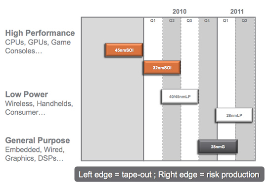
Global Foundries' 2010 - 2011 Manufacturing Roadmap
The problem is that if you follow every last one of these design rules and hints your chip won’t be any faster than it was on the older manufacturing process. Your yield will be about the same but your cost will be higher since you’ll bloat your design taking into account these “hints”.
Generally between process nodes the size of the wafer doesn’t change. We were at 200mm wafers for a while and now modern fabs use 300mm wafers. The transistor size does shrink however, so in theory you could fit more die on a wafer with each process shrink.
The problem is with any new process, the cost per wafer goes up. It’s a new process, most likely more complex, and thus the wafer cost is higher. If the wafer costs are 50% higher, then you need to fit at least 50% more die on each wafer in order to break even with your costs on the old process. In reality you actually need to fit more than 50% die per wafer on the new process because yields usually suck at the start. But if you follow the foundry’s guidelines to guarantee yield, you won’t even be close to breaking even.
The end result is you get zero benefit from moving to the new process. That’s not an option for anyone looking to actually use Moore’s Law to their advantage. Definitely not for a GPU company.
The solution is to have some very smart people in your company that can take these design rules and hints the foundry provides, and figure out which ones can be ignored, and ways to work around the others. This is an area where ATI and NVIDIA differ greatly.


132 Comments
View All Comments
AdiQue - Sunday, February 14, 2010 - link
I fully subscribe to point raised by a few previous posters. Namely, the article being such a worthy read, it actually justifies the creation of an account for the sheer reason of expressing appreciation to your fantastic work, which does stand out in the otherwise well saturated market of technology blogs.geok1ng - Sunday, February 14, 2010 - link
"I almost wonder if AMD’s CPU team could learn from the graphics group's execution. I do hope that along with the ATI acquisition came the open mindedness to learn from one another"it would be a true concern if based on mere observation, but the hard facts are soo much terrible: AMD fired tons of ATI personnel, hence ATI drivers are years behind NVIDIA- we are still begging for centered timings on ATO cards, a feature that NVIDIA offers 6 generations past! ATI produces cards that are gameless. DirectX 10.1?! There was a single game with DirectX 10.1 support, and NVIDIA made the game developer REMOVE DirectX 10.1 features with a game patch that "increased" performance. DirectX 11?! ATI has to put money on driver developing team and spend TONS of cash in game developing.
I would be a happier costumer if the raw performance of my 4870X2 was paired with the seamless driver experience of my previous 8800GT.
And another game that AMD was too late is the netbook and ultralow voltage mobile market. A company with the expertise in integrated graphics and HTPCs GPUs with ZERO market share on this segment?! give me a break!
LordanSS - Monday, February 15, 2010 - link
Funny... after the heaps of problems I had with drivers, stability and whatnot with my old 8800GTS (the original one, 320MB), I decided to switch to ATI with a 4870. Don't regret doing that.My only gripe with my current 5870 is the drivers' and the stupid giant mouse cursor. The Catalyst 9.12 hotfix got rid of it, but it came back on the 10.1.... go figure. Other than that, haven't had problems with it and have been getting great performance.
blackbrrd - Monday, February 15, 2010 - link
I think the reason he had issues with the X2 is that it's a dual card. I think most gfx card driver problems comes from dual cards in any configuration (dual, crossfire, sli)The reason you had issues with the 320mb card is that it had some real issues because of the half-memory. The 320mb cards where cards originally intended as gtx cards, but binned as gts cards that again got binned as 320mb cards instead of 640mb cards. Somehow Nvidia didn't test these cards good enough.
RJohnson - Sunday, February 14, 2010 - link
Please get back under your bridge troll...Warren21 - Sunday, February 14, 2010 - link
Are you kidding me? Become informed before you spread FUD like this. I've been able to choose centered timings in my CCC since I've had my 2900 Pro back in fall 2007. Even today on my CrossFire setup you can still use it.As for your DX10.1 statement, thank NVIDIA for that. You must remember that THEY are the 600lb gorilla of the graphics industry - I fail to see how the exact instance you cite does anything other than prove just that.
As for the DX11 statement, if NVIDIA had it today I bet you'd be singing a different tune. The fact that it's here today is because of Microsoft's schedule which both ATI and NVIDIA follow. NV would have liked nothing more than to have Fermi out in 2009, believe that.
Kjella - Sunday, February 14, 2010 - link
"AMD fired tons of ATI personnel, hence ATI drivers are years behind NVIDIA-"Wow, you got it backwards. The old ATI drivers sucked horribly, they may not be great now either but whatever AMD did or didn't do the drivers have been getting better, not worse.
Scali - Sunday, February 14, 2010 - link
It's a shame that AMD doesn't have its driver department firing on all cylinders like the hardware department is.The 5000-series are still plagued with various annoying bugs, such as the video playback issues you discovered, and the 'gray screen' bug under Windows 7.
Then there's OpenCL, which still hasn't made it into a release driver yet (while nVidia has been winning over many developers with Cuda and PhysX in the meantine, while also offering OpenCL support in release drivers, which support a wider set of features than AMD, and better performance).
And through the months that I've had my 5770 I've noticed various rendering glitches aswell, although most of them seem to have been solved with later driver updates.
And that's just the Windows side. Linux and OS X aren't doing all that great either. FreeBSD isn't even supported at all.
hwhacker - Sunday, February 14, 2010 - link
I don't log in and comment very often, but had to for this article.Anand, these type of articles (Rv770,'Rv870',and SSD) are beyond awesome. I hope it continues for Northern Islands and beyond. Everything from the RV870 jar tidbit to the original die spec to the SunSpotting info. It's great that AMD/ATi allows you to report this information, and that you have the journalistic chops to inquire/write about it. Can not provide enough praise. I hope Kendell and his colleagues (like Henri Richard) continue this awesome 'engineering honesty' PR into the future. The more they share, within understandable reason, the more I believe a person can trust a company and therefore support it.
I love the little dropped hints BTW. Was R600 supposed to be 65nm but early TSMC problems cause it revert to 80nm like was rumored? Was Cypress originally planned as ~1920 shaders (2000?) with a 384-bit bus? Would sideport have helped the scaling issues with Hemlock? I don't know these answers, but the fact all of these things were indirectly addressed (without upsetting AMD) is great to see explored, as it affirms my belief I'm not the only one interested in them. It's great to learn the informed why, not just the unsubstantiated what.
If I may preemptively pose an inquiry, please ask whomever at AMD when NI is briefed if TSMC canceling their 32nm node and moving straight to 28nm had anything to do with redesigns of that chip. There are rumors it caused them to rethink what the largest chip should be, and perhaps revert back to what the original Cypress design (as hinted in this article?) for that chip, causing a delay from Q2-Q3 to Q3-Q4, not unlike the 30-45 day window you mention about redesigning Cypress. I wonder if NI was originally meant to be a straight shrink?
hwhacker - Sunday, February 14, 2010 - link
I meant Carrell above. Not quite sure why I wrote Kendell.