The RV870 Story: AMD Showing up to the Fight
by Anand Lal Shimpi on February 14, 2010 12:00 AM EST- Posted in
- GPUs
What Made it All Ok: 4 GPUs in < 6 Months
Through a lot of hard work and sacrifice, even on Carrell’s part, ATI cut the RV870 from as much as 22mm on a side down to roughly 18mm x 18mm. The problem is that RV770 was around 16mm on a side. The RV870 was still too big.
Carrell wanted to cut it down even more, but two things changed his mind. First, in order to build 870 in the space of a 770 ATI would have to cut out much more from the chip than Carrell originally tought. One of the things that would have to go was some of the shader core.
In order to run the GDDR5 memory at the sort of data rates that ATI was targeting for the 5870 the analog PHYs on the chip had to grow considerably. At 16mm on a side ATI would either have to scale back memory bandwidth or eat into the shader core area. Either way we would’ve had a slower chip.
I asked Carrell if 16mm on a side would’ve made the RV870 $100 cheaper at launch, putting it on par with the RV770 launch prices. He said no. I didn’t find out why until much later, but I’ll save that story for another time.
Sacrificing performance to meet the 16mm x 16mm die size targets wasn’t going to happen, but what ultimately convinced Carrell to go with a larger die this time around was something that ATI didn’t get nearly enough praise for: the ability to launch 4 different 40nm DirectX 11 GPUs in less than 6 months.
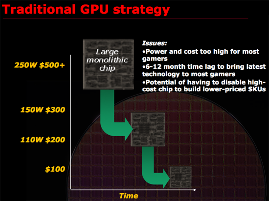
Remember that Carrell’s beef with building the biggest GPU possible is that it takes too long for the majority of customers to get access to derivatives of that GPU. Look at how long it took G80 or GT200 to scale down. And who knows when we’ll see $150 Fermi/GF100 derivatives.
But ATI Engineering promised two things. First, that Cypress would have a successor called Juniper that would be ready around the same time. Secondly, two more GPUs would follow and the whole stack will be done and out in less than 6 months. ATI came close in 2008 with 3 GPUs in 3 months, but the fourth member of the 4000 series didn’t show up until April of 2009.
It wasn’t an impossible feat. ATI does have concurrent design teams and a lot of engineering resources in India/China. By working on Juniper in tandem with Cypress, assuming there were no show stopping bugs, ATI could exploit efficiencies in two teams effectively working on the same hardware (Juniper was just half a Cypress).
The idea of taking such a huge risk made Carrell uncomfortable. Running two GPU designs in parallel, for the same family of chips, is risky. If everything works out perfectly, you get two chips out at the same time. If it doesn’t, you’ve just tied up two design teams on one product generation. A slip here would give ATI its own Fermi.
What ultimately sold Carrell was the fact that engineering told him that they believed they could pull it off. Carrell believes in people. He believes if you expect the best out of those around you, then that’s what you’ll get. He couldn’t reconcile his beliefs with doubting the schedule engineering was feeding him. Carrell nervously signed off and the Evergreen stack was born.
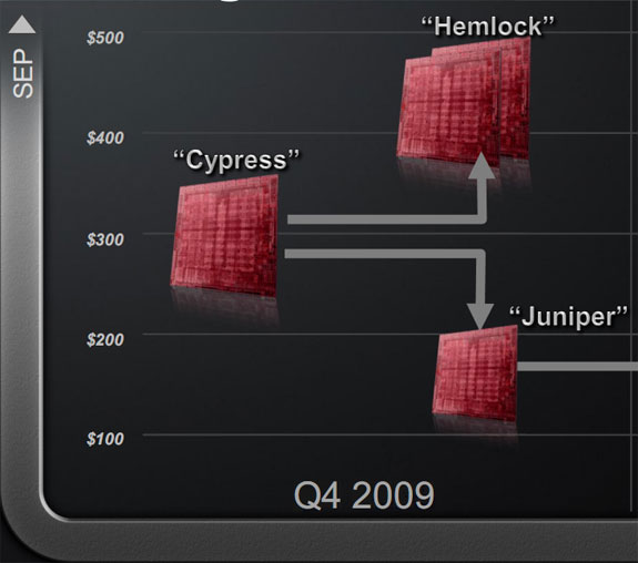
Cypress and Juniper were delivered nearly at the same time. In fact, Juniper was ready a bit earlier and was sampled to developers months before ATI launched the 5000 series. Cedar and Redwood followed, not to mention a dual-Cypress board that became the Radeon HD 5970. And all of this was done and ready in less than 6 months (the chips themselves were all ready within 4 months).
When the smoke cleared ATI had new DirectX 11 parts at $600, $400, $300, $200, $150, $100 and $60. The Windows 7/DirectX 11 market bulge just got serviced.


132 Comments
View All Comments
ImmortalZ - Monday, February 15, 2010 - link
Long time reader and lurker here.This article is one of the best I've read here - hell, it's one of the best I've ever read on any tech site. Reading about and getting perspective on what makes companies like ATI tick is great. Thank you and please, more!
tygrus - Sunday, February 14, 2010 - link
Sequences of numbers in a logical way are easier to remember than names. The RV500, RV600 .. makes order obvious. Using multiple names within a generation of chips are confusing and not memorable. They do not convey sequence or relative complexity.Can you ask if AMD are analysing current games/GPGPU and future games/GPGPU to identify possible areas for improvement or skip less useful proposed design changes. Like the Intel >2% gain for <1% cost.
Yakk - Sunday, February 14, 2010 - link
Excellent article! As I've read in a few other comments, this article (and one similar I'd read prior) made me register for the first time, even if I've been reading this site for many years.I could see why "Behind the scenes" articles can make certain companies nervous and others not, mostly based on their own "corporate culture" I'd think.
It was a very good read, and I'm sure every engineer who worked on any given generation on GPU's could have many stories to tell about tech challenges and baffling (at the time) corporate decisions. And also a manager's side of the work in navigating corporate red tape, working with people, while delivering something worthwhile as an end product is also a huge. Having a good manager (people) with a good subject knowledge (tech) is rare, then for Corp. Execs. to know they have one is MUCH rarer still...
If anyone at AMD/ATI read these comments, PLEASE look at the hardware division and try to implement changes to the software division to match their successes...
(btw been using nv cards almost exclusively since the TNT days, and just got a 5870 for the first time this month. ATI Hardware I'd give an "A+", Software... hmm, I'd give it a "C". Funny thing is nv is almost the exact opposite right now)
Perisphetic - Sunday, February 14, 2010 - link
Someone nominate this man for the Pulitzer Prize!As many have stated before, this is a fantastic article. It goes beyond extraordinary, exceptional and excellent. This has become my new benchmark for high quality computer industry related writing.
Thank you sir.
ritsu - Monday, February 15, 2010 - link
It's not exactly The Soul of a New Machine. But, fine article. It's nice to have a site willing to do this sort of work.shaggart5446 - Sunday, February 14, 2010 - link
very appreciative for this article im from ja but reading this make me file like ill go back to school thanks anand ur the best big up yeah man529th - Sunday, February 14, 2010 - link
The little knowledge I have about the business of making a graphics card, that it was Eyefinity that stunted the stability-growth of the 5xxx drivers by the allocation of resources of the software engineers to make Eyefinity work.chizow - Sunday, February 14, 2010 - link
I usually don't care much for these fluff/PR pieces but this one was pretty entertaining, probably because there was less coverage of what the PR/Marketing guys had to say and more emphasis on the designers and engineers. Carrell sounds like a very interesting guy and a real asset to AMD, they need more innovators like him leading their company and less media exposure from PR talking heads like Chris Hook. Almost tuned out when I saw that intro pic, thankfully the article shifted focus quickly.As for the article itself, among the many interesting points made in there, a few that caught my eye:
1) It sounds like some of the sacrifices made with RV870's die size help explain why it fell short of doubling RV770/790 in terms of performance scaling. Seems as if memory controllers might've also been cut as edge real estate was lost, and happen to be the most glaring case where RV870 specs weren't doubled with regard to RV770.
2) The whole cloak and dagger bit with EyeFinity was very amusing and certainly helps give these soulless tech giants some humanity and color.
3) Also with EyeFinity, I'd probably say Nvidia's solution will ultimately be better, as long as AMD continues to struggle with CrossFire EyeFinity support. It actually seems as if Nvidia is applying the same framebuffer splitting technology via PCIe/SLI link with their recently announced Optimus technology to Nvidia Surround, both of course lending technology from their Quadro line of cards.
4) The discussion about fabs/yields was also very interesting and helps shed some light on some of the differences between the strategies used by both companies in the past to present. AMD has always leveraged new process technologies in the past as soon as possible, Nvidia in the past has more closely followed Intel's Tick/Tock cadence of building high-end on mature processes and teething smaller chips on new processes. That clearly changed this time around on 40nm so it'll be interesting to see what AMD does going forward. I was surprised there wasn't any discussion about why AMD hasn't looked into GlobalFoundries as their GPU foundry.
SuperGee - Sunday, February 14, 2010 - link
nV eyeFinity counter solution is a fast software reaction wich is barly the same thing. You need SLI because one GPU can do only 2 active ports. That the main diference. So you depend on a more high-end platform. A SLI mobo PSU capable of feeding two Gcards. While ATI give yo 3 or 6 ou t of one GPU.nV can deliver something native in there next design. Equal and the possibility to be better at it. But we are still waiting for there DX11 parts. I wonder if they could slap a solution in the refresh or can do only wenn they introduce the new archtecture "GF200".
chizow - Monday, February 15, 2010 - link
Actually EyeFinity's current CF problems are most likely a software problem which is why Nvidia's solution is already superior from a flexibility and scalability standpoint. They've clearly worked out the kinks of running multiple GPUs to a single frame buffer and then redistributing portions of that framebuffer to different GPU outputs.AMD's solution seems to have problems because output on each individual GPU is only downstream atm, so while one GPU can send frame data to a primary GPU for CF, it seems secondary GPUs have problems receiving frame data to output portions of the frame.
Why I say Nvidia's solution is better overall is simply because the necessity of SLI will automatically decrease the chance of a poor gaming experience when gaming at triple resolutions, which is clearly a problem with some newer games and single-GPU EyeFinity. Also, if AMD was able to use multiple card display outputs, it would solve the problem of requiring a $100 active DP dongle for the 3rd output if a user doesn't have a DP capable monitor.